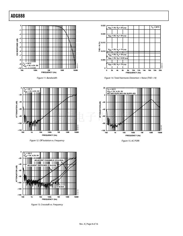
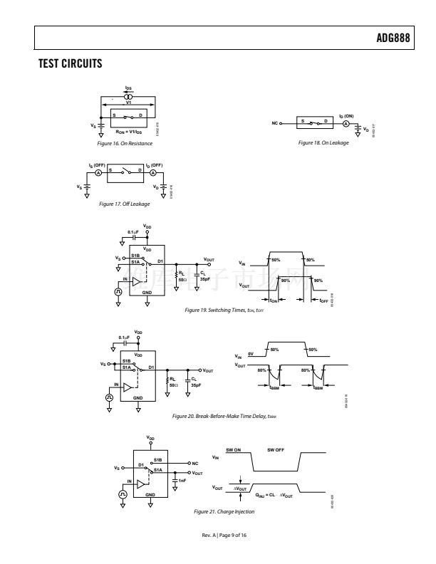
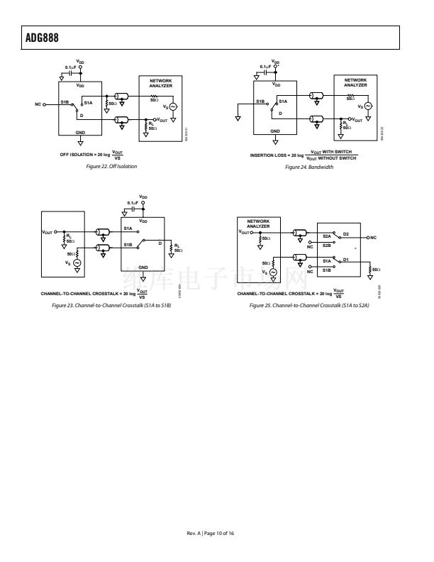
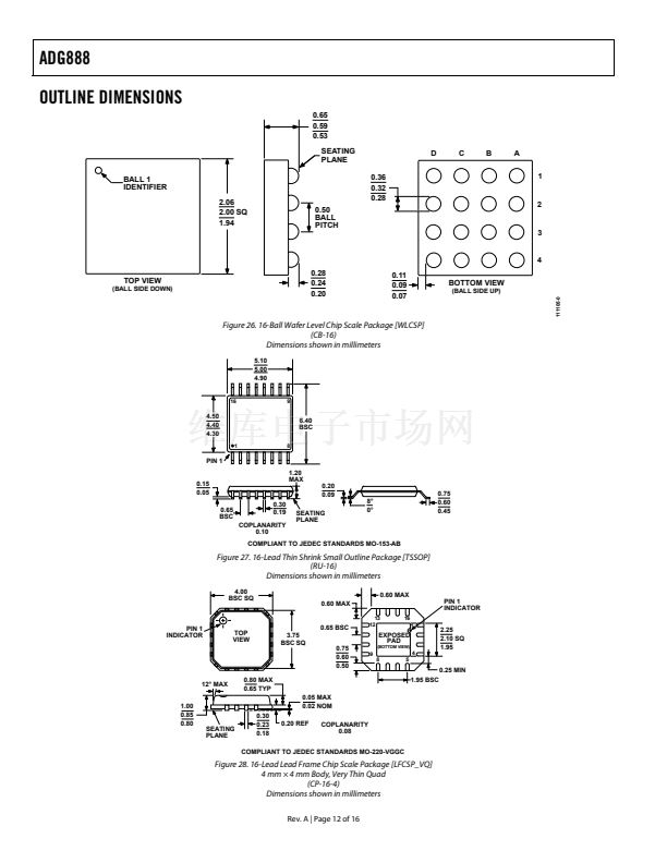
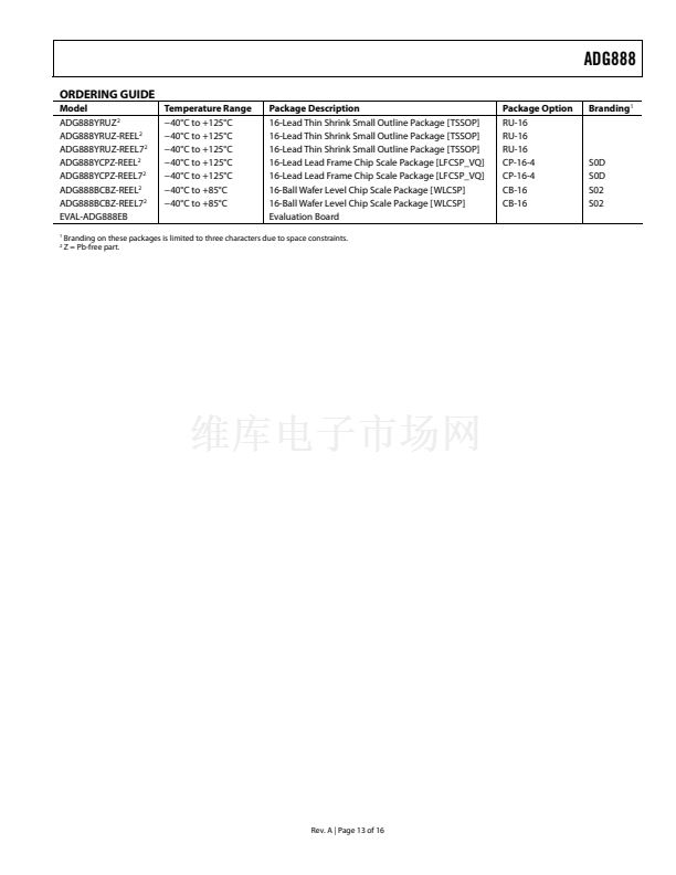
ADG888
ABSOLUTE MAXIMUM RATINGS
T
A
= 25掳C, unless otherwise noted.
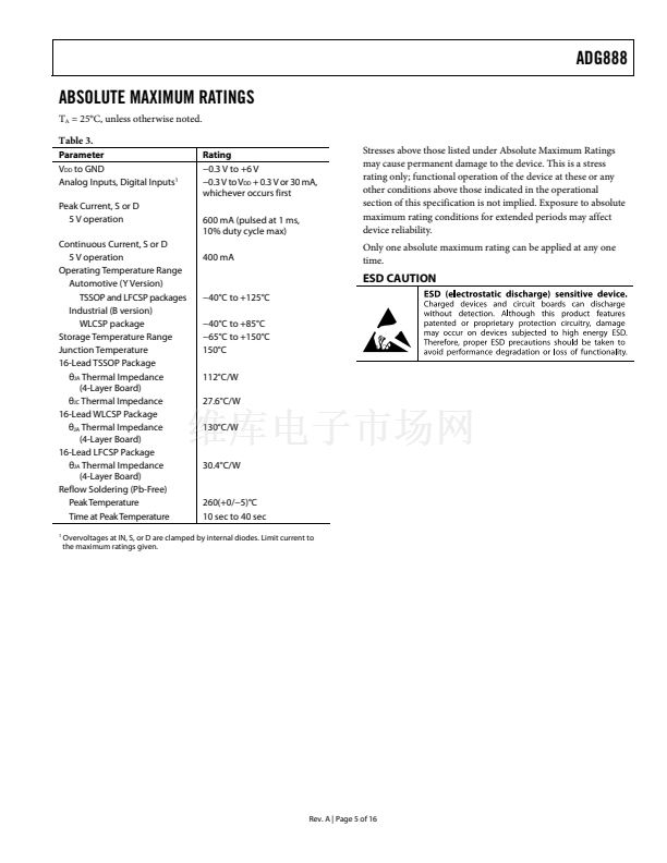
Table 3.
Parameter
V
DD
to GND
Analog Inputs, Digital Inputs
1
Peak Current, S or D
5 V operation
Continuous Current, S or D
5 V operation
Operating Temperature Range
Automotive (Y Version)
TSSOP and LFCSP packages
Industrial (B version)
WLCSP package
Storage Temperature Range
Junction Temperature
16-Lead TSSOP Package
胃
JA
Thermal Impedance
(4-Layer Board)
胃
JC
Thermal Impedance
16-Lead WLCSP Package
胃
JA
Thermal Impedance
(4-Layer Board)
16-Lead LFCSP Package
胃
JA
Thermal Impedance
(4-Layer Board)
Reflow Soldering (Pb-Free)
Peak Temperature
Time at Peak Temperature
1
Rating
鈭?.3 V to +6 V
鈭?.3 V to V
DD
+ 0.3 V or 30 mA,
whichever occurs first
600 mA (pulsed at 1 ms,
10% duty cycle max)
400 mA
Stresses above those listed under Absolute Maximum Ratings
may cause permanent damage to the device. This is a stress
rating only; functional operation of the device at these or any
other conditions above those indicated in the operational
section of this specification is not implied. Exposure to absolute
maximum rating conditions for extended periods may affect
device reliability.
Only one absolute maximum rating can be applied at any one
time.
ESD CAUTION
鈭?0掳C to +125掳C
鈭?0掳C to +85掳C
鈭?5掳C to +150掳C
150掳C
112掳C/W
27.6掳C/W
130掳C/W
30.4掳C/W
260(+0/鈭?)掳C
10 sec to 40 sec
Overvoltages at IN, S, or D are clamped by internal diodes. Limit current to
the maximum ratings given.
Rev. A | Page 5 of 16


 1
1
 2
2
 3
3
 4
4
 5
5
 6
6
 7
7
 8
8
 9
9
 10
10
 11
11
 12
12
 13
13
 14
14
 15
15
 16
16
