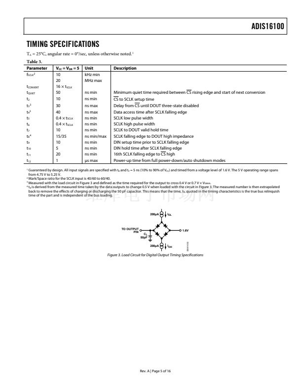
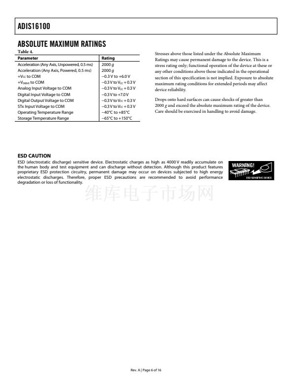
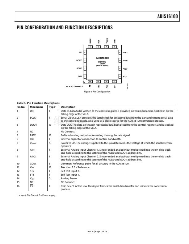
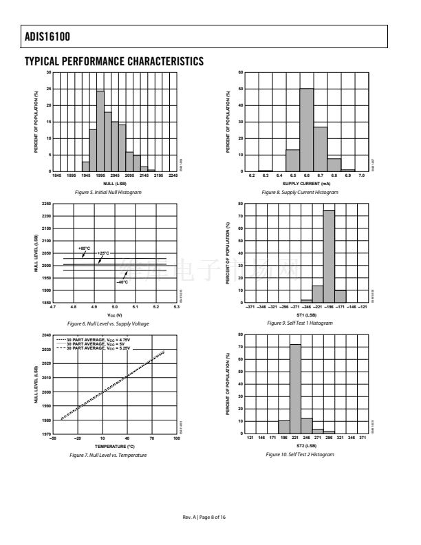
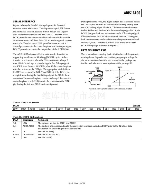
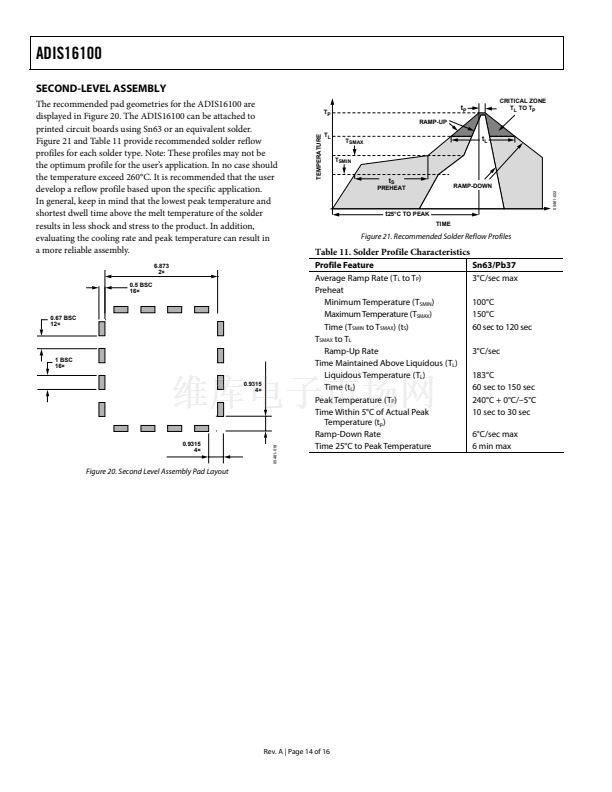
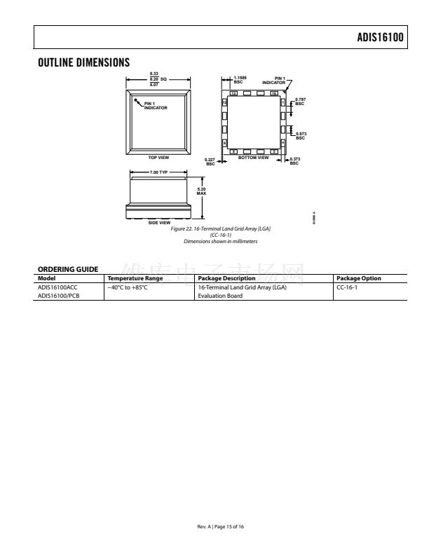
ADIS16100
THEORY OF OPERATION
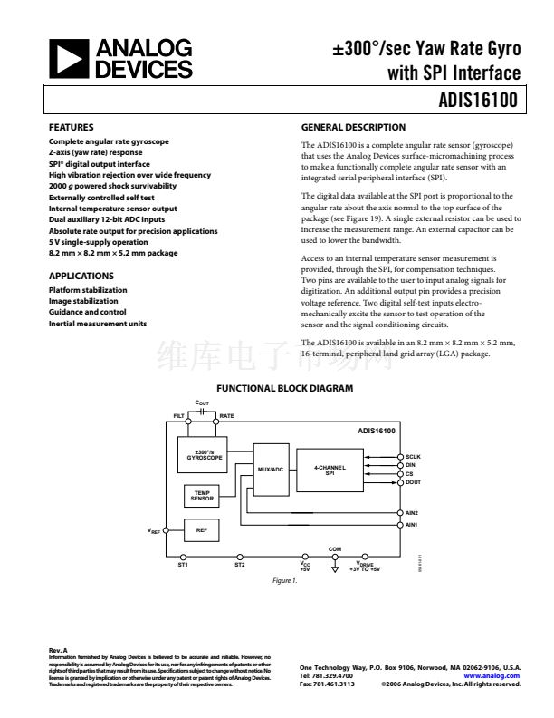
The ADIS16100 operates on the principle of a resonator gyro.
Two polysilicon sensing structures each contain a dither frame,
which is electrostatically driven to resonance. This produces the
necessary velocity element to produce a Coriolis force during
angular rate. At two of the outer extremes of each frame, orthogo-
nal to the dither motion, are movable fingers that are placed
between fixed pickoff fingers to form a capacitive pickoff structure
that senses Coriolis motion. The resulting signal is fed to a series
of gain and demodulation stages that produce the electrical rate
signal output. The rate signal is then converted to a digital
representation of the output on the SPI pins. The dual-sensor
design rejects external
g-forces
and vibration. Fabricating the
sensor with the signal conditioning electronics preserves signal
integrity in noisy environments.
The electrostatic resonator requires 14 V to 16 V for operation.
Because only 5 V is typically available in most applications, a
charge pump is included on-chip.
After the demodulation stage, there is a single-pole, low-pass
filter included on-chip that is used to limit high frequency
artifacts before final amplification. A second single-pole, low-
pass filter is set up via the bandwidth limit capacitor, C
OUT
. This
pole acts as the primary filter within the system (see the Increasing
Measurement Range section).
The trade-off associated with increasing the full-scale range are
potential increase in output null drift (as much as 2掳/sec over
temperature) and introducing initial null bias errors that must
be calibrated.
SETTING BANDWIDTH
The ADIS16100 provides the ability to reduce the bandwidth.
This important feature enables a simple method for achieving
optimal bandwidth/noise trade-offs. An external capacitor can
be used in combination with an on-chip resistor to create a low-
pass filter to limit the bandwidth of the ADIS16100鈥檚 rate response.
The 鈭? dB frequency is defined as
f
OUT
=
1/
(
2
脳
蟺
脳
R
OUT
脳
(
C
OUT
+
0.022 渭F
))
where
R
OUT
represents an internal impedance that was trimmed
during manufacturing to 180 k惟 卤 1%.
Any external resistor applied between the RATE pin and the
FILT pin results in
R
OUT
=
(
180 k惟
脳
R
EXT
)
/
(
180 k惟
+
R
EXT
)
With C
OUT
= 0 渭F, a default 鈭? dB frequency response of 40 Hz
is obtained, based upon an internal 0.022 渭F capacitor imple-
mented on-chip.
SUPPLY AND COMMON CONSIDERATIONS
Power supply noise and transient behaviors can influence the
accuracy and stability of any sensor-based measurement system.
When considering the power supply for the ADIS16100, it is
important to understand that the ADIS16100 provides 0.2 渭F of
decoupling capacitance on the V
CC
pin. Depending on the level
of noise present in the system power supply, the ADIS16100
may not require any additional decoupling capacitance for this
supply. The analog supply, V
CC
, and the digital drive supply,
V
DRIVE
, are segmented to allow multiple logic levels to be used in
receiving the digital output data. V
DRIVE
is intended for the
down-stream logic power supply and supports standard 3.3 V
and 5 V logic families. The V
DRIVE
supply does not have internal
decoupling capacitors.
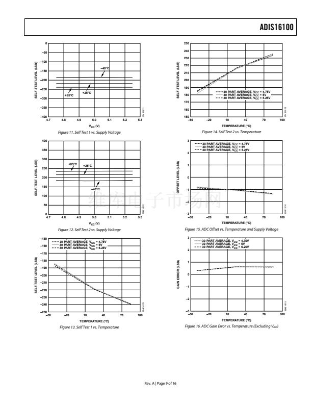
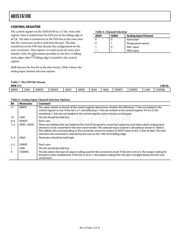
SELF-TEST FUNCTION
The ADIS16100 includes a self-test feature that actuates each of
the sensing structures and associated electronics in the same
manner, as if subjected to angular rate. It provides a simple
method for exercising the mechanical structure of the sensor,
along with the entire signal processing circuit. It is activated by
standard logic high levels applied to Input ST1, Input ST2, or
both. ST1 causes a change in the digital output equivalent to
typically 鈭?21 LSB, and ST2 causes an opposite +221 LSB
change. The self-test response follows the viscosity temperature
dependence of the package atmosphere, approximately
0.25%/掳C.
Activating both ST1 and ST2 simultaneously is not damaging.
Because ST1 and ST2 are not necessarily closely matched,
actuating both simultaneously can result in an apparent null
bias shift.
INCREASING MEASUREMENT RANGE
The full-scale measurement range of the ADIS16100 is increased
by placing an external resistor between the RATE pin and the
FILT pin. This external resistor would be in parallel with an
internal 180 k惟, 1% resistor. For example, a 330 k惟 external
resistor gives ~50% increase in the full-scale range. This is
effective for up to a 4脳 increase in the full-scale range
(minimum value of the parallel resistor allowed is 45 k惟). The
internal circuitry headroom requirements prevent further
increase in the linear full-scale output range.
CONTINUOUS SELF TEST
As an additional failure detection measure, power-on self test
can be performed. However, some applications warrant a
continuous self test-while-sensing rate.
Rev. A | Page 11 of 16


 1
1
 2
2
 3
3
 4
4
 5
5
 6
6
 7
7
 8
8
 9
9
 10
10
 11
11
 12
12
 13
13
 14
14
 15
15
 16
16
