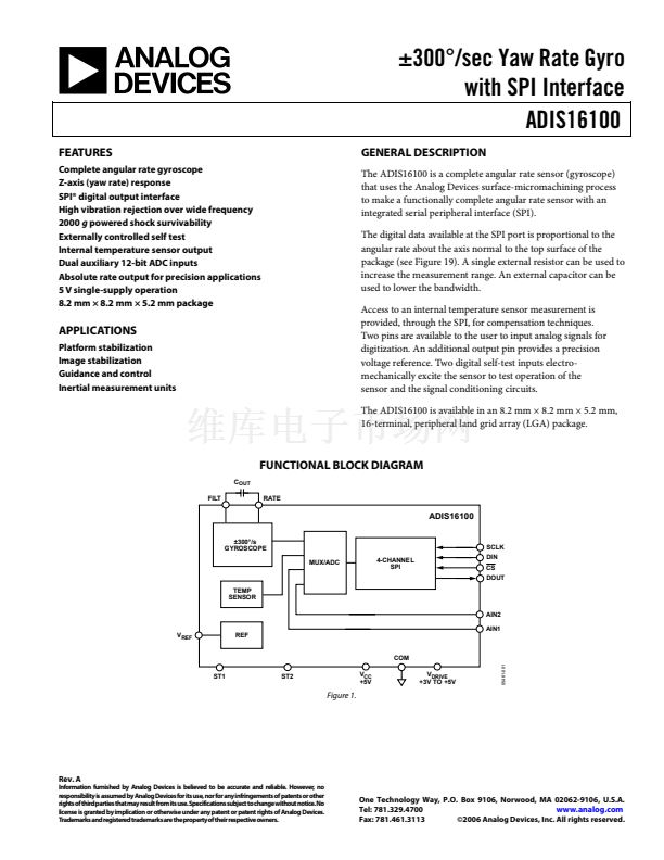
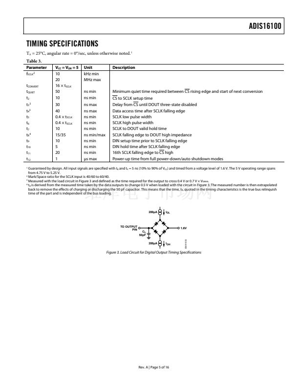
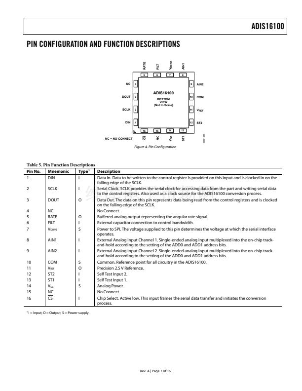
ADIS16100
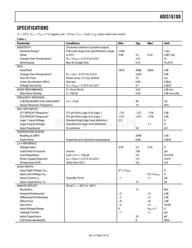
SERIAL INTERFACE
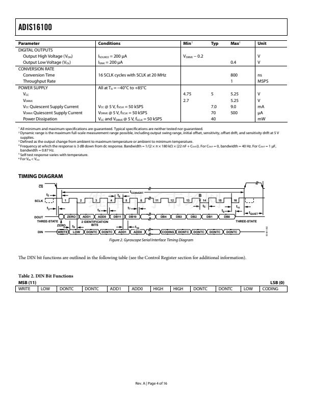
Figure 2 shows the detailed timing diagram for the serial
interface to the ADIS16100. The chip select signal, CS, frames
the entire data transfer, because it must be kept in a Logic 0
state to communicate with the ADIS16100. The serial clock,
SCLK, provides the conversion clock and controls the transfer
of information to and from the ADIS16100 during each conver-
sion cycle. The data input, DIN, provides access to critical
control parameters in the control register, and the output signal,
DOUT, provides access to the output data of the ADIS16100.
The ADIS16100 offers an efficient data transfer function by
supporting simultaneous READ and WRITE cycles. A data
transfer cycle is started when the CS transitions to a Logic 0
state. If DIN is in Logic 1 state during the first falling edge of
the SCLK, then the next 11 SCLK cycles fill the control register
with the contents on the DIN pin. The appropriate bit definitions
for DIN can be found in Table 7 and Table 8. If the DIN is in
a Logic 0 state during the first falling edge of the SCLK, then
contents of the control register remain unchanged. Because the
control register is only 12-bits wide, the contents on the DIN
pin during the last four SCLK cycles are ignored.
During this same cycle, the digital output data is clocked out on
the DOUT pin, with the bit transitions occurring shortly after
the SCLK falling edges. The DOUT bit sequence is character-
ized in Table 9 and Table 10. On the 16th falling edge of SCLK, the
DOUT line goes back into a three-state mode. If the rising edge of
CS occurs before 16 SCLKs have elapsed, the DOUT line goes
back into three-state mode and the control register is not updated.
Otherwise, DOUT returns to a three-state mode on the 16th
SCLK falling edge, as shown in Figure 2.
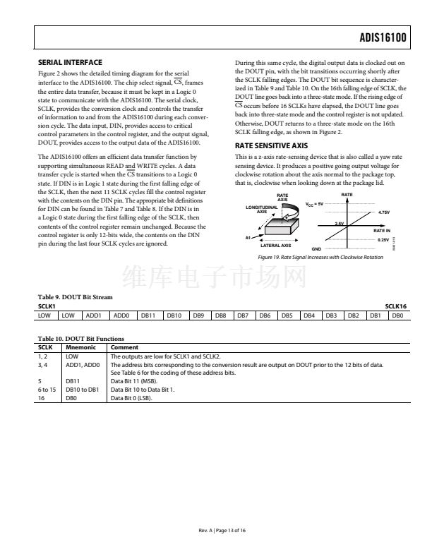
RATE SENSITIVE AXIS
This is a z-axis rate-sensing device that is also called a yaw rate
sensing device. It produces a positive going output voltage for
clockwise rotation about the axis normal to the package top,
that is, clockwise when looking down at the package lid.
RATE
AXIS
LONGITUDINAL
AXIS
V
CC
= 5V
4.75V
2.5V
RATE IN
0.25V
LATERAL AXIS
GND
05461-019
RATE
A1
Figure 19. Rate Signal Increases with Clockwise Rotation
Table 9. DOUT Bit Stream
SCLK1
LOW
LOW
ADD1
ADD0
DB11
DB10
DB9
DB8
DB7
DB6
DB5
DB4
DB3
DB2
SCLK16
DB1
DB0
Table 10. DOUT Bit Functions
SCLK
1, 2
3, 4
5
6 to 15
16
Mnemonic
LOW
ADD1, ADD0
DB11
DB10 to DB1
DB0
Comment
The outputs are low for SCLK1 and SCLK2.
The address bits corresponding to the conversion result are output on DOUT prior to the 12 bits of data.
See Table 6 for the coding of these address bits.
Data Bit 11 (MSB).
Data Bit 10 to Data Bit 1.
Data Bit 0 (LSB).
Rev. A | Page 13 of 16


 1
1
 2
2
 3
3
 4
4
 5
5
 6
6
 7
7
 8
8
 9
9
 10
10
 11
11
 12
12
 13
13
 14
14
 15
15
 16
16
