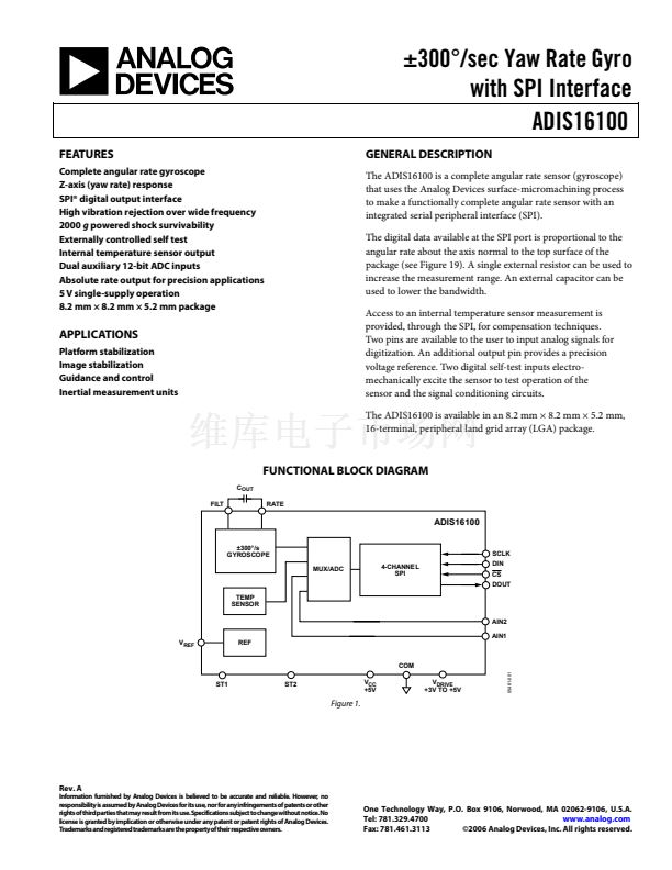
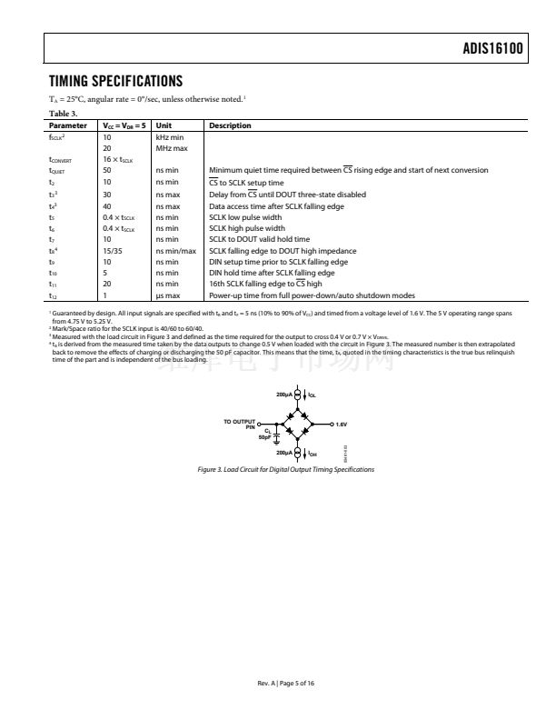
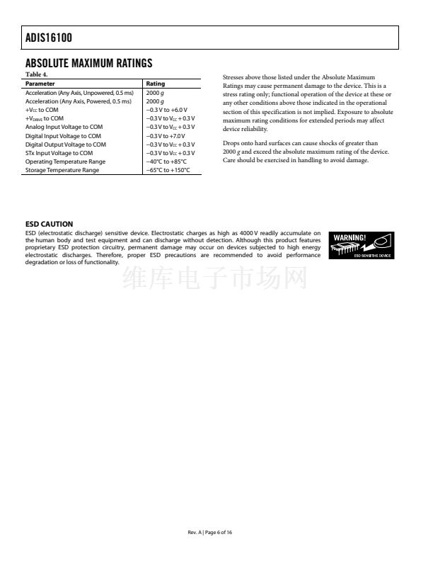
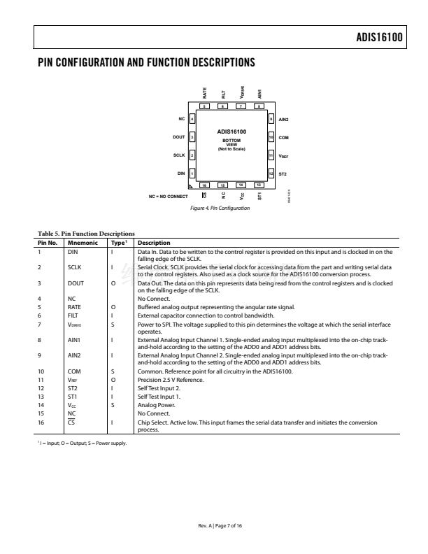
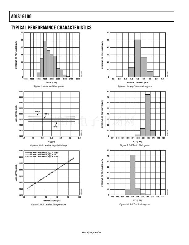
ADIS16100
Parameter
DIGITAL OUTPUTS
Output High Voltage (V
OH
)
Output Low Voltage (V
OL
)
CONVERSION RATE
Conversion Time
Throughput Rate
POWER SUPPLY
V
CC
V
DRIVE
V
CC
Quiescent Supply Current
V
DRIVE
Quiescent Supply Current
Power Dissipation
1
2
Conditions
I
SOURCE
= 200 渭A
I
SINK
= 200 渭A
16 SCLK cycles with SCLK at 20 MHz
All at T
A
= 鈭?0掳C to +85掳C
Min
1
V
DRIVE
鈭?0.2
Typ
Max
1
Unit
V
V
ns
MSPS
V
V
mA
渭A
mW
0.4
800
1
4.75
2.7
5
7.0
70
40
5.25
5.25
9.0
500
V
CC
@ 5 V, f
SCLK
= 50 kSPS
V
DRIVE
@ 5 V, f
SCLK
= 50 kSPS
V
CC
and V
DRIVE
@ 5 V, f
SCLK
= 50 kSPS
All minimum and maximum specifications are guaranteed. Typical specifications are neither tested nor guaranteed.
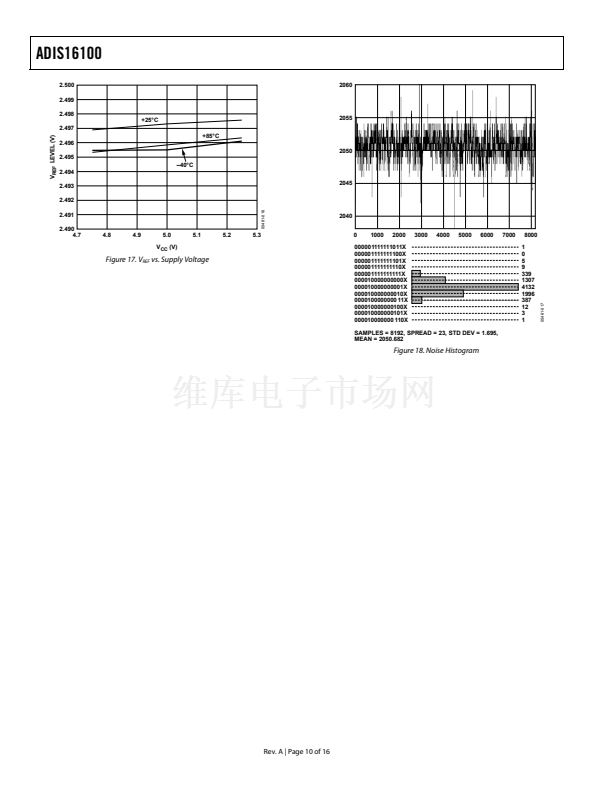
Dynamic range is the maximum full-scale measurement range possible, including output swing range, initial offset, sensitivity, offset drift, and sensitivity drift at 5 V
supplies.
3
Defined as the output change from ambient to maximum temperature or ambient to minimum temperature.
4
Frequency at which the response is 3 dB down from dc response. Bandwidth = 1/(2 脳 蟺 脳 180 k惟 脳 (22 nF + C
OUT
)). For C
OUT
= 0, bandwidth = 40 Hz. For C
OUT
= 1 渭F,
bandwidth = 0.87 Hz.
5
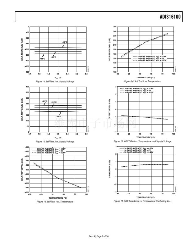
Self-test response varies with temperature.
6
For V
IN
< V
CC
.
TIMING DIAGRAM
CS
t
2
SCLK
1
2
3
4
t
6
5
t
CONVERT
6
11
12
13
B
14
15
16
t
3
ZERO
DOUT
THREE-STATE
ZERO
t
9
t
4
ADD1
ADD0
DB11
2 IDENTIFICATION
BITS
DONTC
DONTC
ADD1
t
7
DB10
DB4
DB3
DB2
t
5
t
8
DB1
DB0
t
11
t
QUIET
THREE-STATE
05461-002
t
10
ADD0
CODING
DONTC
DONTC
DONTC
DONTC
DIN
WRITE
LOW
Figure 2. Gyroscope Serial Interface Timing Diagram
The DIN bit functions are outlined in the following table (see the Control Register section for additional information).
Table 2. DIN Bit Functions
MSB (11)
WRITE
LOW
DONTC
DONTC
ADD1
ADD0
HIGH
HIGH
DONTC
DONTC
LOW
LSB (0)
CODING
Rev. A | Page 4 of 16


 1
1
 2
2
 3
3
 4
4
 5
5
 6
6
 7
7
 8
8
 9
9
 10
10
 11
11
 12
12
 13
13
 14
14
 15
15
 16
16
