ADG714/ADG715
鈥?0
V
DD
= 5V
T
A
= 25 C
鈥?0
GENERAL DESCRIPTION
ATTENUATION 鈥?dB
鈥?0
鈥?0
The ADG714 and ADG715 are serially controlled, octal SPST
switches, controlled by either a 2- or 3-wire interface. Each bit
of the 8-bit serial word corresponds to one switch of the part. A
Logic 1 in the particular bit position turns on the switch, while a
Logic 0 turns the switch off. Because each switch is independently
controlled by an individual bit, this provides the option of having
any, all, or none of the switches ON.
When changing the switch conditions, a new 8-bit word is writ-
ten to the input shift register. Some of the bits may be the same
as the previous write cycle, as the user may not wish to change
the state of some switches. In order to minimize glitches on the
output of these switches, the part cleverly compares the state of
switches from the previous write cycle. If the switch is already
in the ON condition, and is required to stay ON, there will be
minimal glitches on the output of the switch.
POWER-ON RESET
鈥?0
鈥?0
鈥?00
30k
100k
1M
FREQUENCY 鈥?Hz
10M
100M
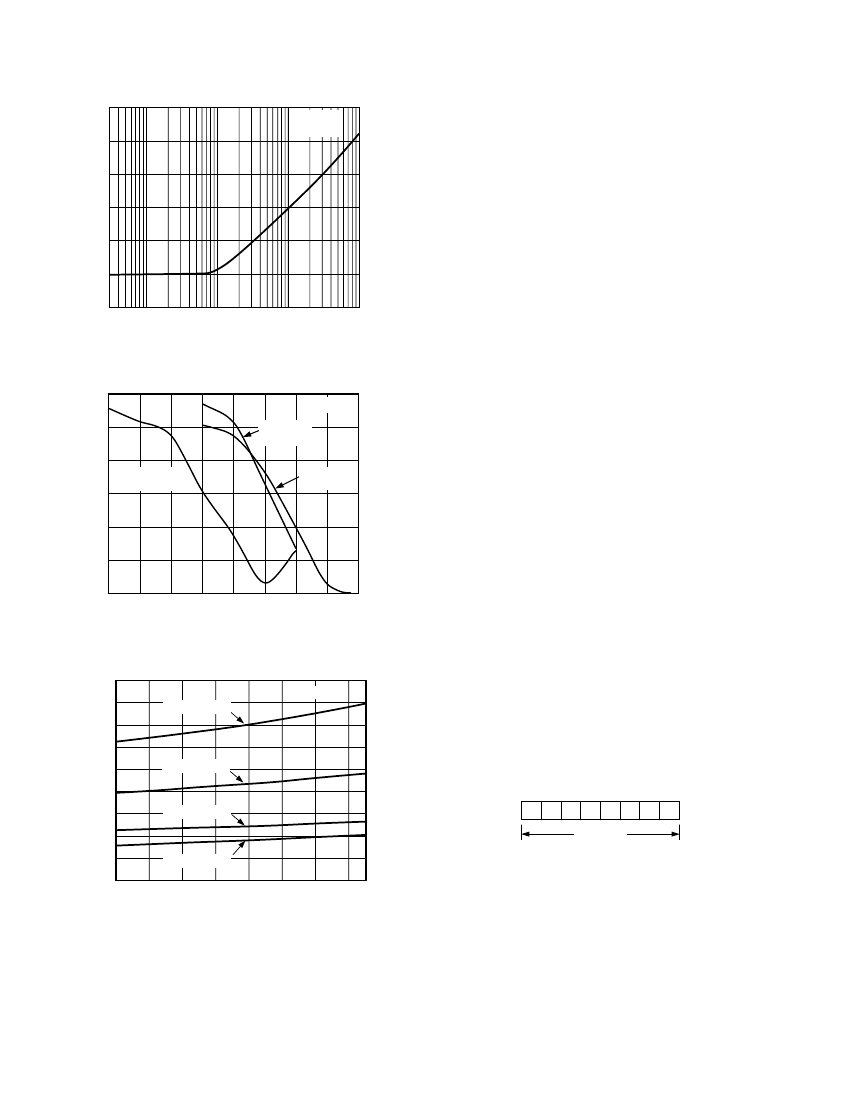
Figure 15. Crosstalk vs. Frequency
10
T
A
= 25 C
5
V
DD
= +3.3V
V
SS
= GND
On power-up of the device, all switches will be in the OFF con-
dition and the internal shift register is 铿乴led with zeros and will
remain so until a valid write takes place.
SERIAL INTERFACE
3-Wire Serial Interface
0
Q
INJ
鈥?pC
V
DD
= +3.0V
V
SS
= 鈥?.0V
鈥?
V
DD
= +5V
V
SS
= GND
鈥?0
The ADG714 has a 3-wire serial interface (SYNC, SCLK, and
DIN), that is compatible with SPI, QSPI, MICROWIRE
interface standards and most DSPs. Figure 1 shows the tim-
ing diagram of a typical write sequence.
Data is written to the 8-bit shift register via DIN under the con-
trol of the
SYNC
and SCLK signals. Data may be written to
the shift register in more or less than eight bits. In each case
the shift register retains the last eight bits that were written.
When
SYNC
goes low, the input shift register is enabled. Data
from DIN is clocked into the shift register on the falling edge of
SCLK. Each bit of the 8-bit word corresponds to one of the eight
switches. Figure 18 shows the contents of the input shift regis-
ter. Data appears on the DOUT pin on the rising edge of SCLK
suitable for daisy chaining, delayed of course by eight bits. When
all eight bits have been written into the shift register, the
SYNC
line is brought high again. The switches are updated with the
new con铿乬uration and the input shift register is disabled. With
SYNC
held high, the input shift register is disabled, so further data
or noise on the DIN line will have no effect on the shift register.
DB7 (MSB)
DB0 (LSB)
S6
S5
S4
S3
S2
S1
鈥?5
鈥?0
鈥?
鈥?
鈥?
0
1
2
VOLTAGE 鈥?V
3
4
5
Figure 16. Charge Injection vs. Source/Drain Voltage
45
V
SS
= GND
40
35
30
T
O N
, V
DD
= 3V
TIME 鈥?ns
25
20
15
10
5
0
10
T
O N
, V
DD
= 5V
T
OFF
, V
DD
= 3V
S8
S7
DATA BITS
T
O F F
, V
DD
= 5V
20
30
40
50
60
TEMPERATURE 鈥?C
70
80
Figure 18. Input Shift Register Contents
SERIAL INTERFACE
2-Wire Serial Interface
Figure 17. T
ON
/T
OFF
Times vs. Temperature for ADG714
The ADG715 is controlled via an I
2
C-compatible serial bus.
This device is connected to the bus as a slave device (no clock is
generated by the switch).
The ADG715 has a 7-bit slave address. The 铿乿e MSBs are 10010
and the two LSBs are determined by the state of the A0 and
A1 pins.
prev
next
