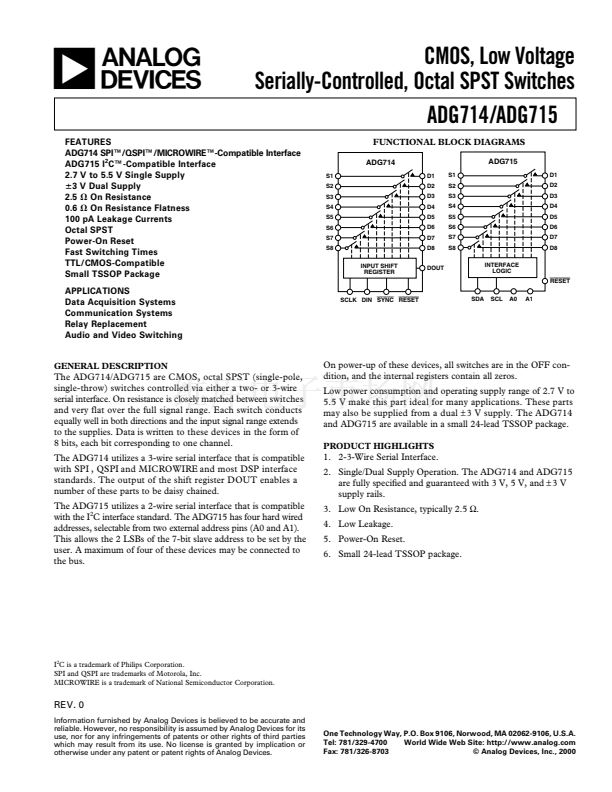
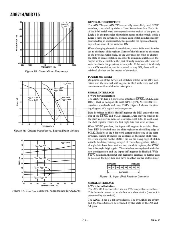
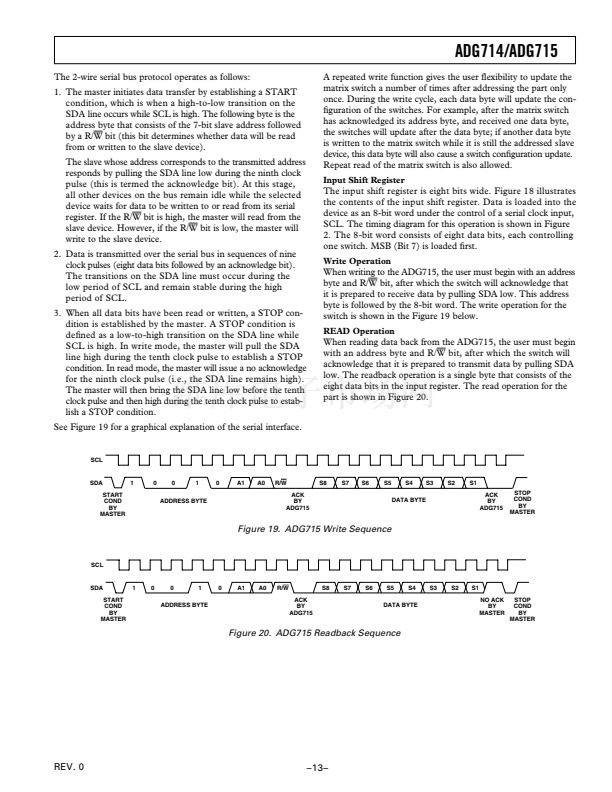
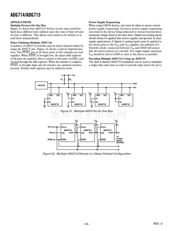
ADG714/ADG715
The 2-wire serial bus protocol operates as follows:
1. The master initiates data transfer by establishing a START
condition, which is when a high-to-low transition on the
SDA line occurs while SCL is high. The following byte is the
address byte that consists of the 7-bit slave address followed
by a R/W bit (this bit determines whether data will be read
from or written to the slave device).
The slave whose address corresponds to the transmitted address
responds by pulling the SDA line low during the ninth clock
pulse (this is termed the acknowledge bit). At this stage,
all other devices on the bus remain idle while the selected
device waits for data to be written to or read from its serial
register. If the R/W bit is high, the master will read from the
slave device. However, if the R/W bit is low, the master will
write to the slave device.
2. Data is transmitted over the serial bus in sequences of nine
clock pulses (eight data bits followed by an acknowledge bit).
The transitions on the SDA line must occur during the
low period of SCL and remain stable during the high
period of SCL.
3. When all data bits have been read or written, a STOP con-
dition is established by the master. A STOP condition is
de铿乶ed as a low-to-high transition on the SDA line while
SCL is high. In write mode, the master will pull the SDA
line high during the tenth clock pulse to establish a STOP
condition. In read mode, the master will issue a no acknowledge
for the ninth clock pulse (i.e., the SDA line remains high).
The master will then bring the SDA line low before the tenth
clock pulse and then high during the tenth clock pulse to estab-
lish a STOP condition.
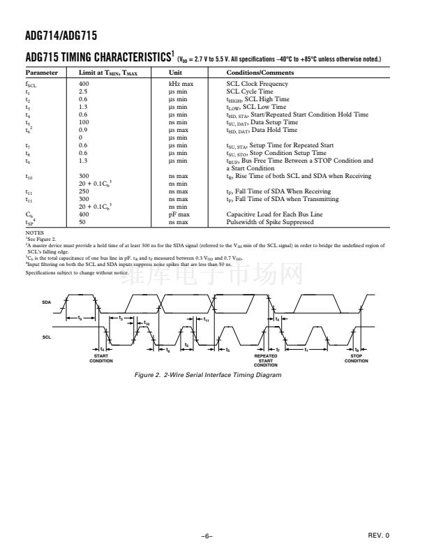
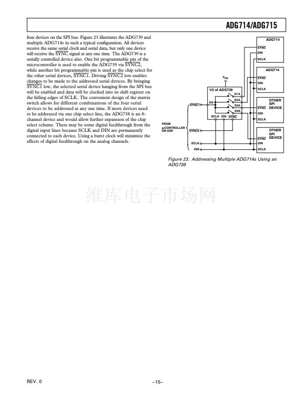
See Figure 19 for a graphical explanation of the serial interface.
A repeated write function gives the user flexibility to update the
matrix switch a number of times after addressing the part only
once. During the write cycle, each data byte will update the con-
铿乬uration of the switches. For example, after the matrix switch
has acknowledged its address byte, and received one data byte,
the switches will update after the data byte; if another data byte
is written to the matrix switch while it is still the addressed slave
device, this data byte will also cause a switch con铿乬uration update.
Repeat read of the matrix switch is also allowed.
Input Shift Register
The input shift register is eight bits wide. Figure 18 illustrates
the contents of the input shift register. Data is loaded into the
device as an 8-bit word under the control of a serial clock input,
SCL. The timing diagram for this operation is shown in Figure
2. The 8-bit word consists of eight data bits, each controlling
one switch. MSB (Bit 7) is loaded 铿乺st.
Write Operation
When writing to the ADG715, the user must begin with an address
byte and R/W bit, after which the switch will acknowledge that
it is prepared to receive data by pulling SDA low. This address
byte is followed by the 8-bit word. The write operation for the
switch is shown in the Figure 19 below.
READ Operation
When reading data back from the ADG715, the user must begin
with an address byte and R/W bit, after which the switch will
acknowledge that it is prepared to transmit data by pulling SDA
low. The readback operation is a single byte that consists of the
eight data bits in the input register. The read operation for the
part is shown in Figure 20.
SCL
SDA
START
COND
BY
MASTER
1
0
0
1
0
A1
A0
R/W
ACK
BY
ADG715
S8
S7
S6
S5
S4
DATA BYTE
S3
S2
S1
ACK
BY
ADG715
STOP
COND
BY
MASTER
ADDRESS BYTE
Figure 19. ADG715 Write Sequence
SCL
SDA
START
COND
BY
MASTER
1
0
0
1
0
A1
A0
R/W
ACK
BY
ADG715
S8
S7
S6
S5
S4
S3
S2
S1
NO ACK
BY
MASTER
STOP
COND
BY
MASTER
ADDRESS BYTE
DATA BYTE
Figure 20. ADG715 Readback Sequence
REV. 0
鈥?3鈥?/div>
prev
next


 1
1
 2
2
 3
3
 4
4
 5
5
 6
6
 7
7
 8
8
 9
9
 10
10
 11
11
 12
12
 13
13
 14
14
 15
15
 16
16
