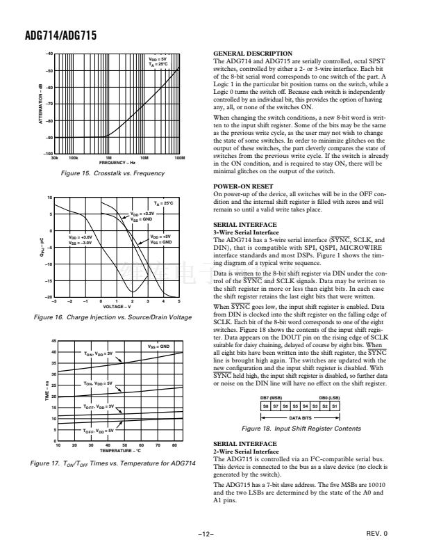
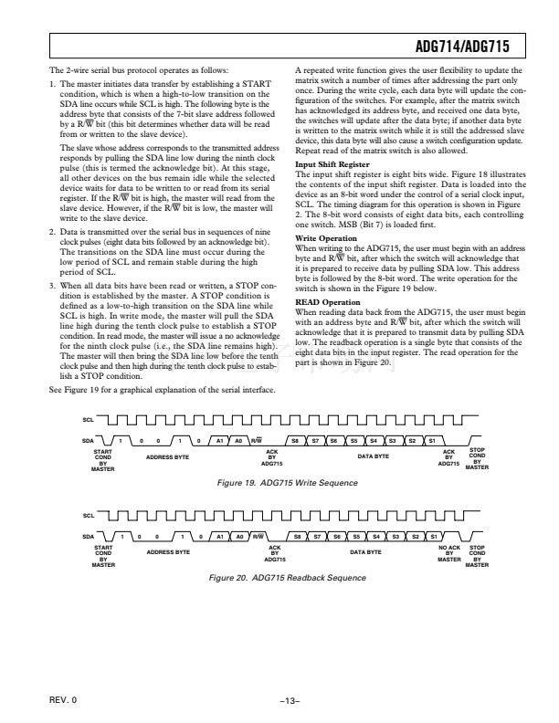
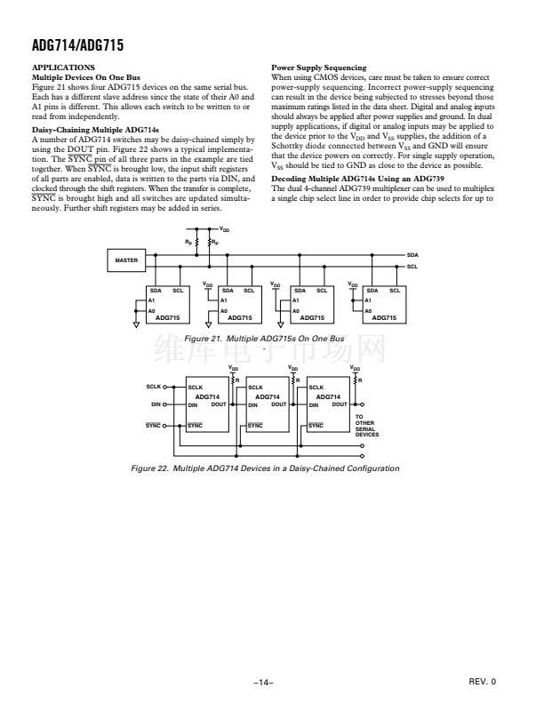
ADG714/ADG715
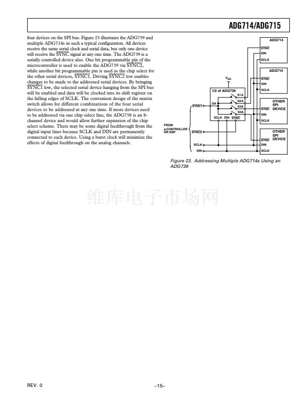
APPLICATIONS
Multiple Devices On One Bus
Power Supply Sequencing
Figure 21 shows four ADG715 devices on the same serial bus.
Each has a different slave address since the state of their A0 and
A1 pins is different. This allows each switch to be written to or
read from independently.
Daisy-Chaining Multiple ADG714s
A number of ADG714 switches may be daisy-chained simply by
using the DOUT pin. Figure 22 shows a typical implementa-
tion. The
SYNC
pin of all three parts in the example are tied
together. When
SYNC
is brought low, the input shift registers
of all parts are enabled, data is written to the parts via DIN, and
clocked through the shift registers. When the transfer is complete,
SYNC
is brought high and all switches are updated simulta-
neously. Further shift registers may be added in series.
V
DD
R
P
MASTER
R
P
When using CMOS devices, care must be taken to ensure correct
power-supply sequencing. Incorrect power-supply sequencing
can result in the device being subjected to stresses beyond those
maximum ratings listed in the data sheet. Digital and analog inputs
should always be applied after power supplies and ground. In dual
supply applications, if digital or analog inputs may be applied to
the device prior to the V
DD
and V
SS
supplies, the addition of a
Schottky diode connected between V
SS
and GND will ensure
that the device powers on correctly. For single supply operation,
V
SS
should be tied to GND as close to the device as possible.
Decoding Multiple ADG714s Using an ADG739
The dual 4-channel ADG739 multiplexer can be used to multiplex
a single chip select line in order to provide chip selects for up to
SDA
SCL
V
DD
SDA
A1
A0
SCL
SDA
A1
A0
SCL
V
DD
SDA
A1
A0
SCL
V
DD
SDA
A1
A0
SCL
ADG715
ADG715
ADG715
ADG715
Figure 21. Multiple ADG715s On One Bus
-
V
DD
R
SCLK
DIN
SCLK
SCLK
V
DD
R
SCLK
V
DD
R
ADG714
DIN
DOUT
ADG714
DIN
DOUT
ADG714
DIN
DOUT
TO
OTHER
SERIAL
DEVICES
SYNC
SYNC
SYNC
SYNC
Figure 22. Multiple ADG714 Devices in a Daisy-Chained Con铿乬uration
prev
next


 1
1
 2
2
 3
3
 4
4
 5
5
 6
6
 7
7
 8
8
 9
9
 10
10
 11
11
 12
12
 13
13
 14
14
 15
15
 16
16
