ADG714/ADG715
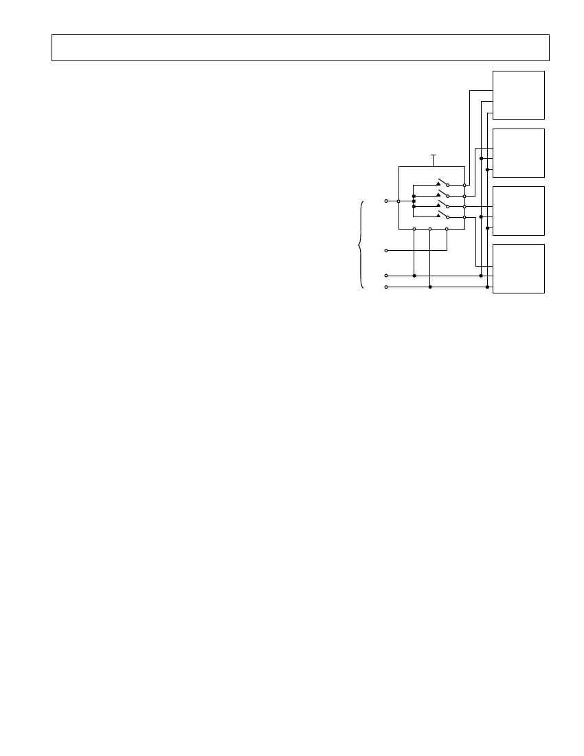
four devices on the SPI bus. Figure 23 illustrates the ADG739 and
multiple ADG714s in such a typical configuration. All devices
receive the same serial clock and serial data, but only one device
will receive the
SYNC
signal at any one time. The ADG739 is a
serially controlled device also. One bit programmable pin of the
microcontroller is used to enable the ADG739 via
SYNC2,
while another bit programmable pin is used as the chip select for
the other serial devices,
SYNC1.
Driving
SYNC2
low enables
changes to be made to the addressed serial devices. By bringing
SYNC1
low, the selected serial device hanging from the SPI bus
will be enabled and data will be clocked into its shift register on
the falling edges of SCLK. The convenient design of the matrix
switch allows for different combinations of the four serial
devices to be addressed at any one time. If more devices need
to be addressed via one chip select line, the ADG738 is an 8-
channel device and would allow further expansion of the chip
select scheme. There may be some digital feedthrough from the
digital input lines because SCLK and DIN are permanently
connected to each device. Using a burst clock will minimize the
effects of digital feedthrough on the analog channels.
ADG714
SYNC
DIN
SCLK
ADG714
V
DD
SYNC
DIN
1/2 of ADG739
S1A
DA
S2A
S3A
S4A
SCLK DIN
SYNC
FROM
CONTROLLER
OR DSP
SCLK
SYNC1
OTHER
SPI
SYNC
DEVICE
DIN
SCLK
SYNC2
OTHER
SPI
SYNC
DEVICE
DIN
SCLK
SCLK
DIN
Figure 23. Addressing Multiple ADG714s Using an
ADG739
REV. 0
鈥?5鈥?/div>
prev
next
