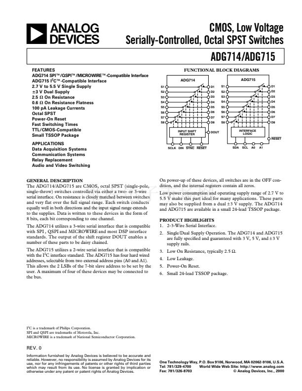
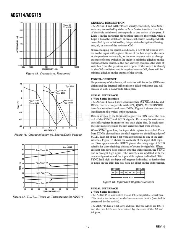
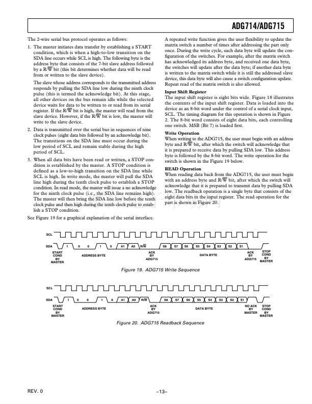
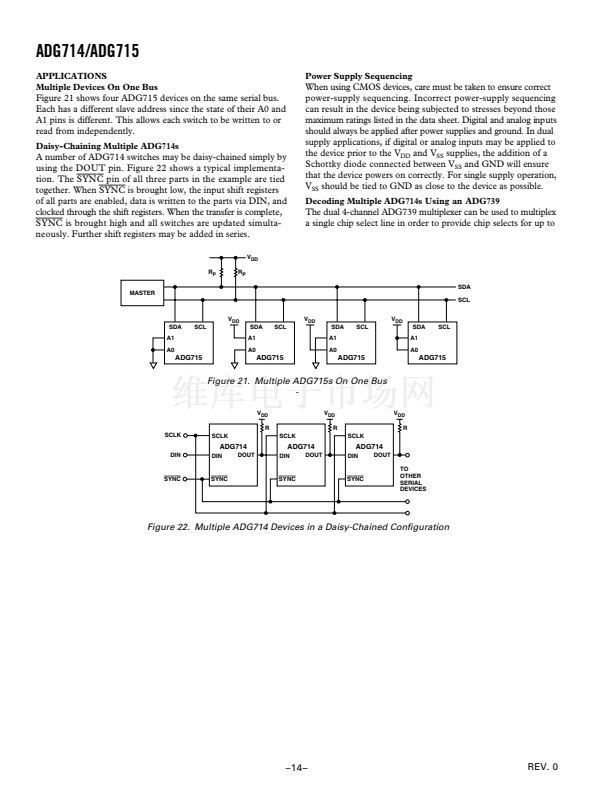
ADG714/ADG715
ADG714 TIMING CHARACTERISTICS
1, 2
(V
Parameter
f
SCLK
t
1
t
2
t
3
t
4
t
5
t
6
t
7
t
8
t
9 3
Limit at T
MIN
, T
MAX
30
33
13
13
0
5
4.5
0
33
20
DD
= 2.7 V to 5.5 V. All speci铿乧ations 鈥?0 C to +85 C unless otherwise noted.)
Conditions/Comments
SCLK Cycle Frequency
SCLK Cycle Time
SCLK High Time
SCLK Low Time
SYNC
to SCLK Rising Edge Setup Time
Data Setup Time
Data Hold Time
SCLK Falling Edge to
SYNC
Rising Edge
Minimum
SYNC
High Time
SCLK Rising Edge to DOUT Valid
Unit
MHz max
ns min
ns min
ns min
ns min
ns min
ns min
ns min
ns min
ns min
NOTES
1
See Figure 1.
2
All input signals are speci铿乪d with tr = tf = 5 ns (10% to 90% of V
DD
) and timed from a voltage level of (V
IL
+ V
IH
)/2.
3
C
L
= 20 pF, R
L
= 1 k鈩?
Speci铿乧ations subject to change without notice.
t
1
SCLK
t
8
t
4
SYNC
t
2
t
3
t
7
t
6
t
5
DIN
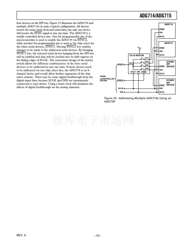
DB7
DB0
t
9
DOUT
DB7
1
DB6
1
DB2
1
DB1
1
DB0
1
NOTE
1
DATA FROM PREVIOUS WRITE CYCLE
Figure 1. 3-Wire Serial Interface Timing Diagram
REV. 0
鈥?鈥?/div>
prev
next


 1
1
 2
2
 3
3
 4
4
 5
5
 6
6
 7
7
 8
8
 9
9
 10
10
 11
11
 12
12
 13
13
 14
14
 15
15
 16
16
