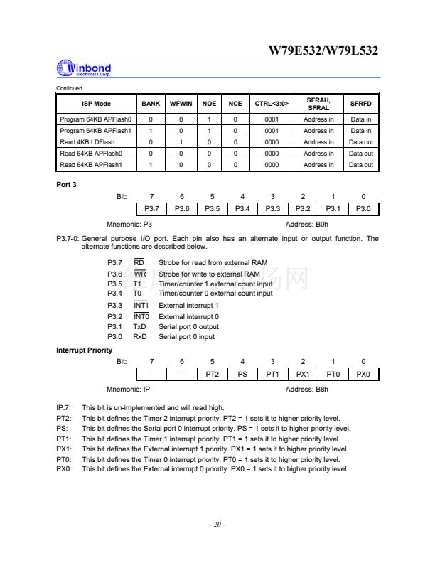
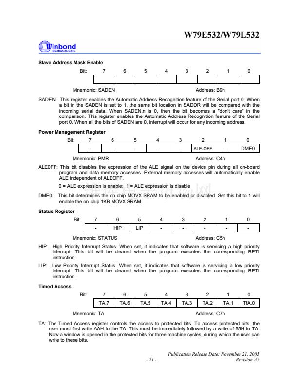
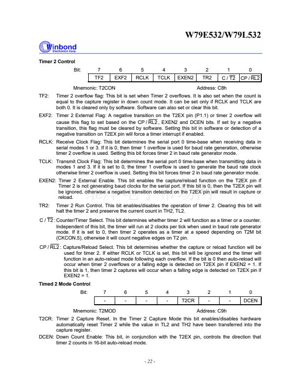
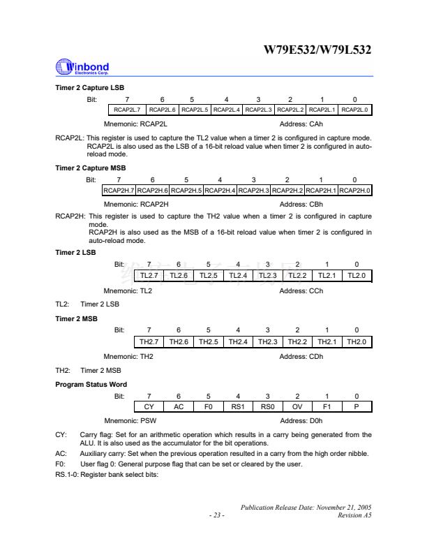
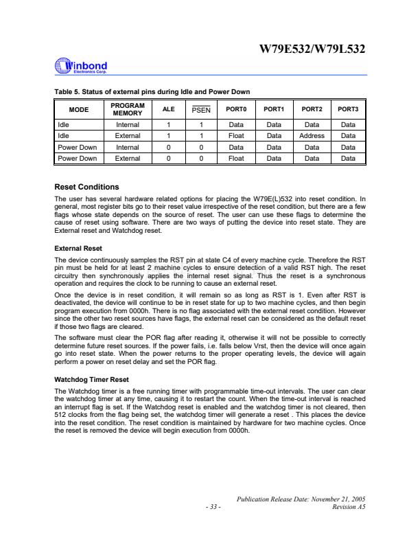
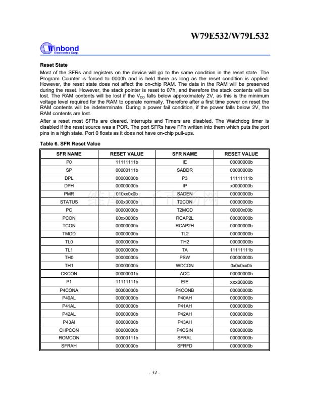
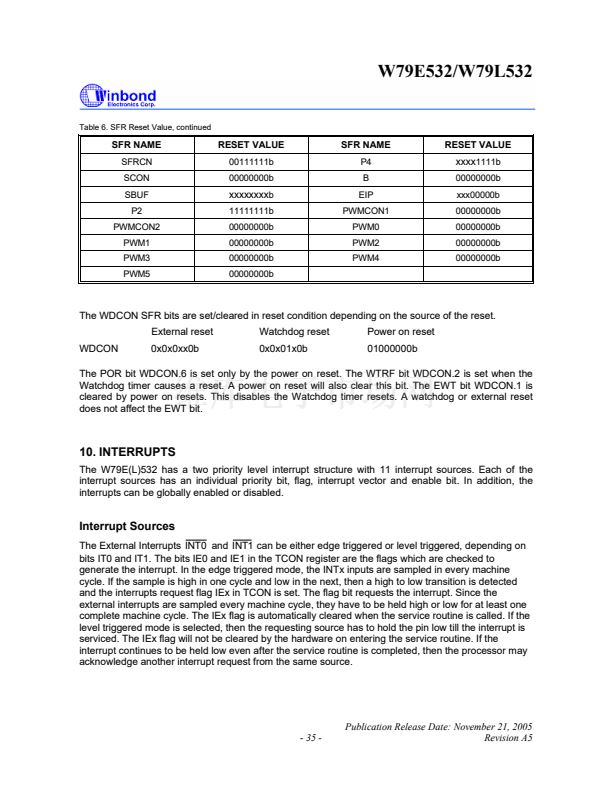
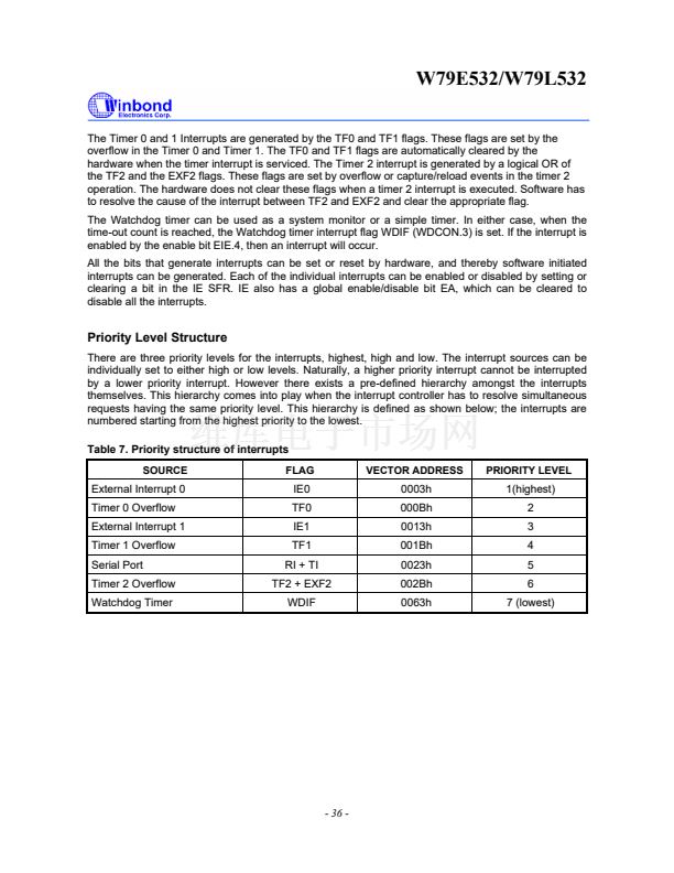
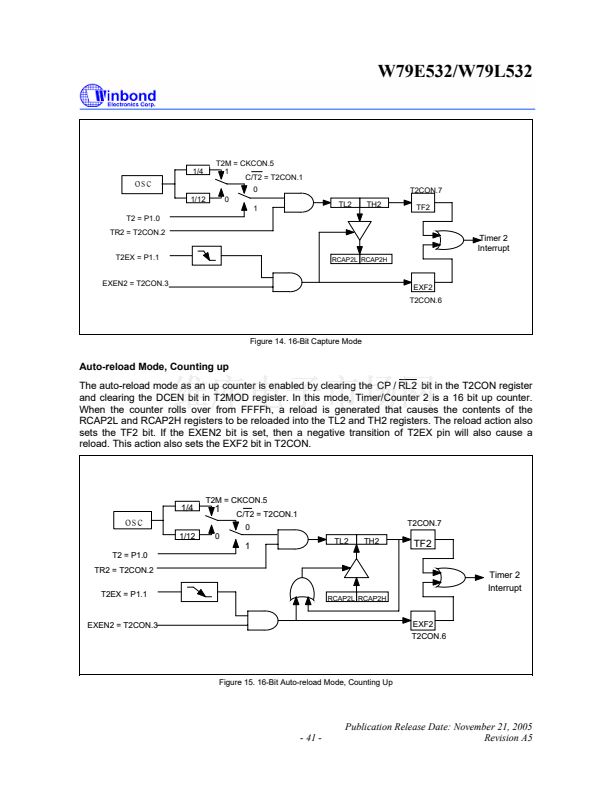
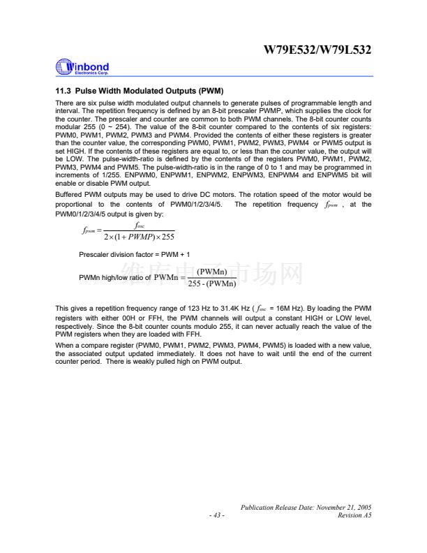
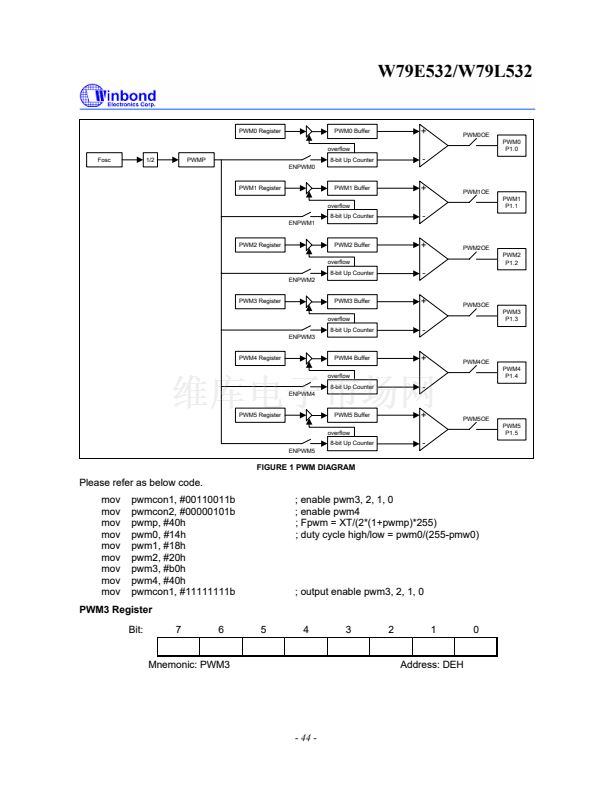
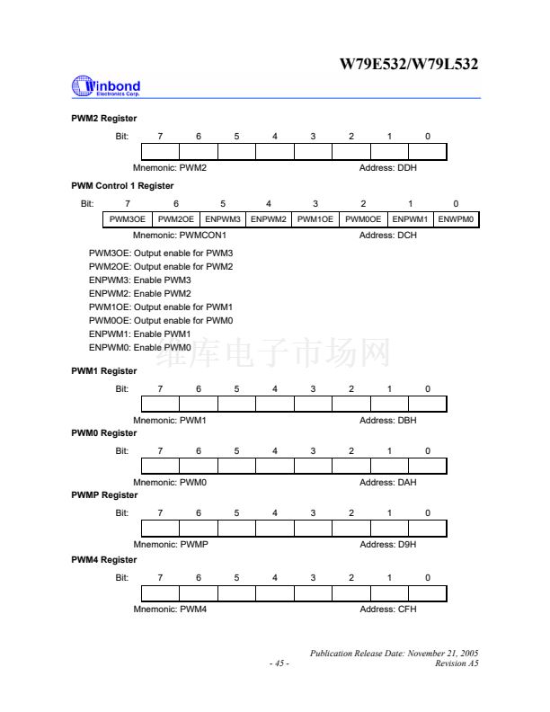
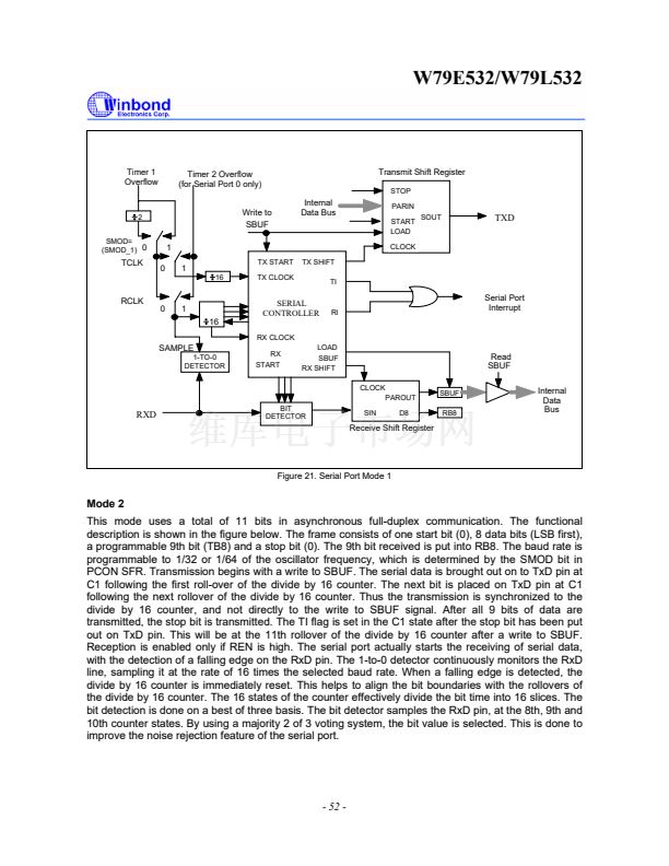
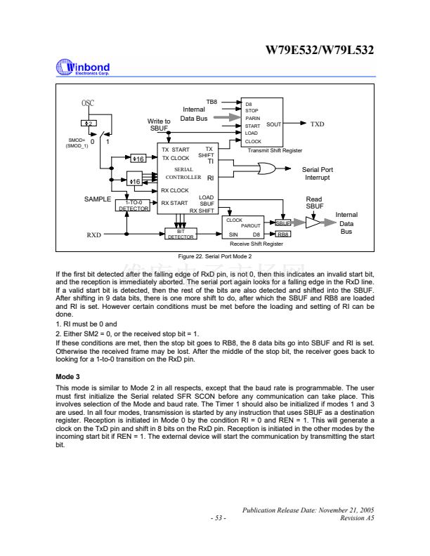
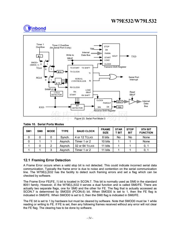
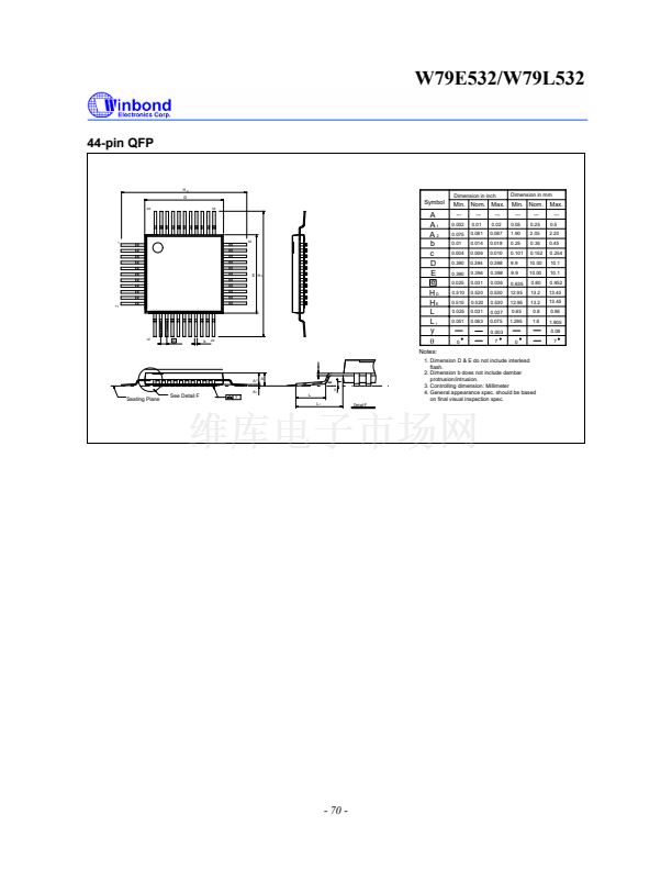
W79E532/W79L532
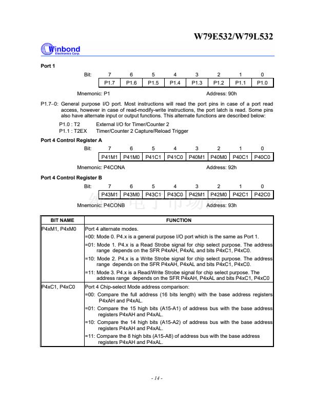
Port 1
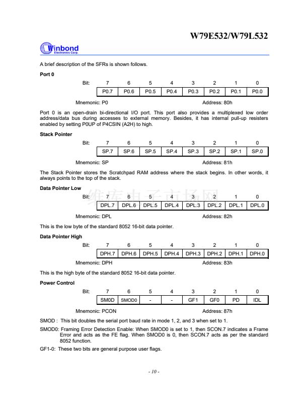
Bit:
7
P1.7
Mnemonic: P1
6
P1.6
5
P1.5
4
P1.4
3
P1.3
2
P1.2
1
P1.1
0
P1.0
Address: 90h
P1.7鈭?: General purpose I/O port. Most instructions will read the port pins in case of a port read
access, however in case of read-modify-write instructions, the port latch is read. Some pins
also have alternate input or output functions. This alternate functions are described below:
P1.0 : T2
P1.1 : T2EX
External I/O for Timer/Counter 2
Timer/Counter 2 Capture/Reload Trigger
Port 4 Control Register A
Bit:
7
P41M1
6
P41M0
5
P41C1
4
P41C0
3
P40M1
2
P40M0
1
P40C1
0
P40C0
Mnemonic: P4CONA
Port 4 Control Register B
Bit:
7
P43M1
6
P43M0
5
P43C1
4
P43C0
3
P42M1
Address: 92h
2
P42M0
1
P42C1
0
P42C0
Mnemonic: P4CONB
BIT NAME
FUNCTION
Address: 93h
P4xM1, P4xM0
Port 4 alternate modes.
=00: Mode 0. P4.x is a general purpose I/O port which is the same as Port 1.
=01: Mode 1. P4.x is a Read Strobe signal for chip select purpose. The address
range depends on the SFR P4xAH, P4xAL and bits P4xC1, P4xC0.
=10: Mode 2. P4.x is a Write Strobe signal for chip select purpose. The address
range depends on the SFR P4xAH, P4xAL and bits P4xC1, P4xC0.
=11: Mode 3. P4.x is a Read/Write Strobe signal for chip select purpose. The
address range depends on the SFR P4xAH, P4xAL and bits P4xC1, P4xC0
P4xC1, P4xC0
Port 4 Chip-select Mode address comparison:
=00: Compare the full address (16 bits length) with the base address registers
P4xAH and P4xAL.
=01: Compare the 15 high bits (A15-A1) of address bus with the base address
registers P4xAH and P4xAL.
=10: Compare the 14 high bits (A15-A2) of address bus with the base address
registers P4xAH and P4xAL.
=11: Compare the 8 high bits (A15-A8) of address bus with the base address
registers P4xAH and P4xAL.
- 14 -


 1
1
 2
2
 3
3
 4
4
 5
5
 6
6
 7
7
 8
8
 9
9
 10
10
 11
11
 12
12
 13
13
 14
14
 15
15
 16
16
 17
17
 18
18
 19
19
 20
20
 21
21
 22
22
 23
23
 24
24
 25
25
 26
26
 27
27
 28
28
 29
29
 30
30
 31
31
 32
32
 33
33
 34
34
 35
35
 36
36
 37
37
 38
38
 39
39
 40
40
 41
41
 42
42
 43
43
 44
44
 45
45
 46
46
 47
47
 48
48
 49
49
 50
50
 51
51
 52
52
 53
53
 54
54
 55
55
 56
56
 57
57
 58
58
 59
59
 60
60
 61
61
 62
62
 63
63
 64
64
 65
65
 66
66
 67
67
 68
68
 69
69
 70
70
 71
71
 72
72
 73
73
 74
74
 75
75
 76
76
 77
77
