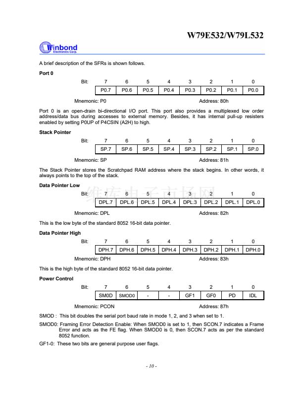
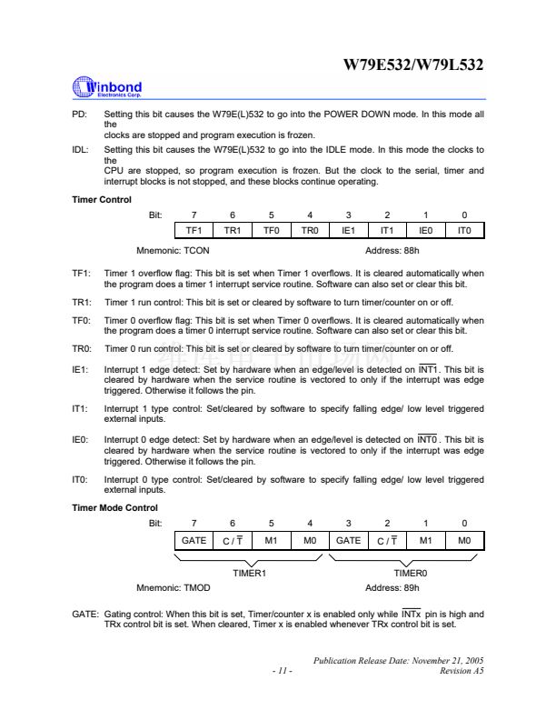
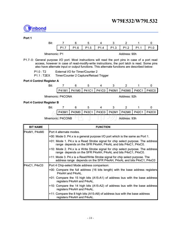
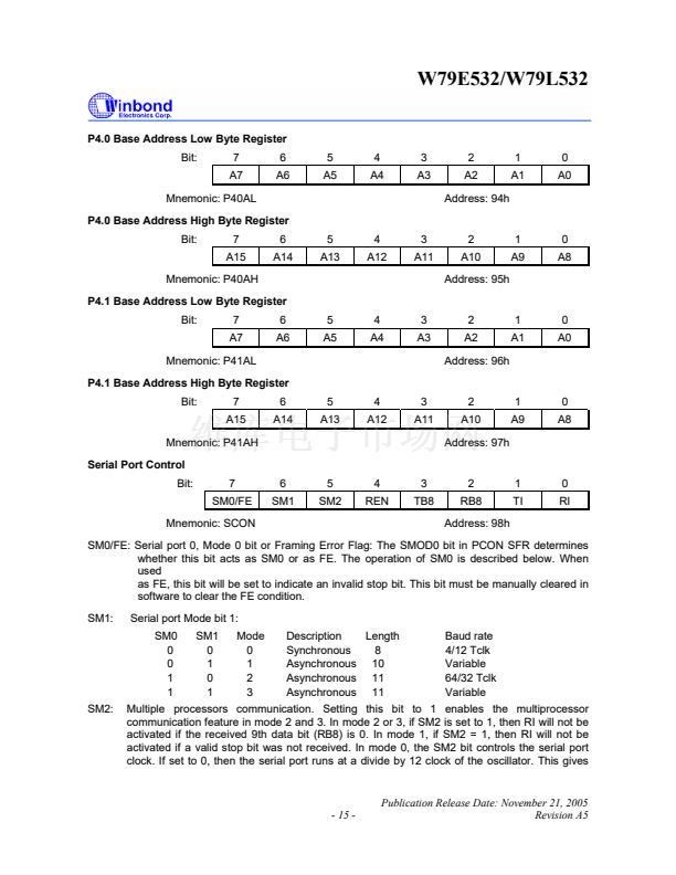
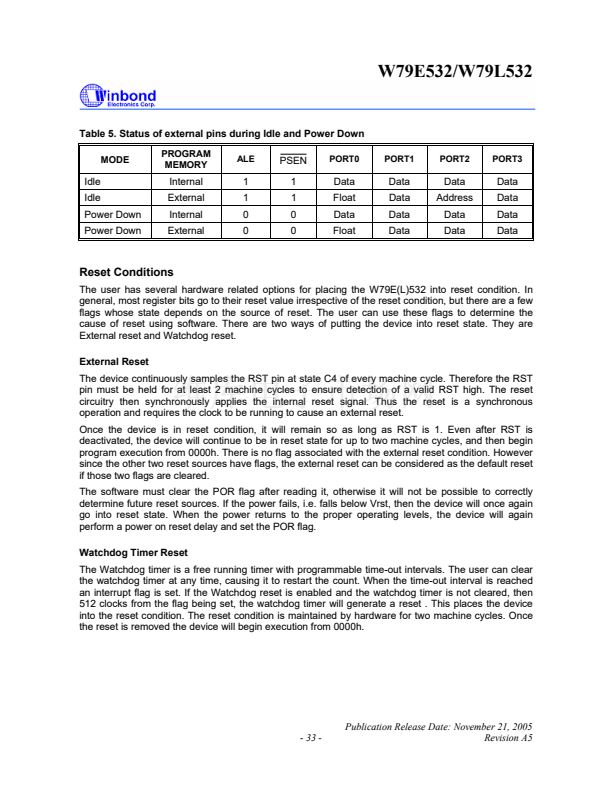
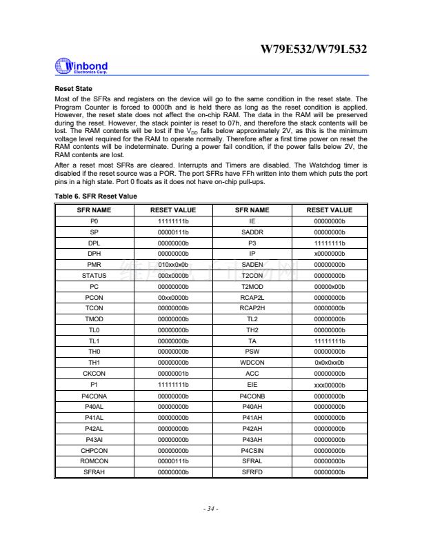
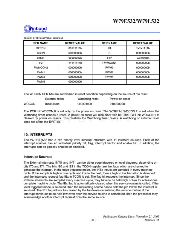
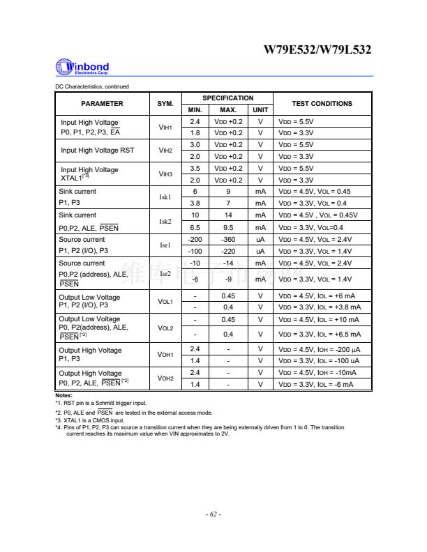
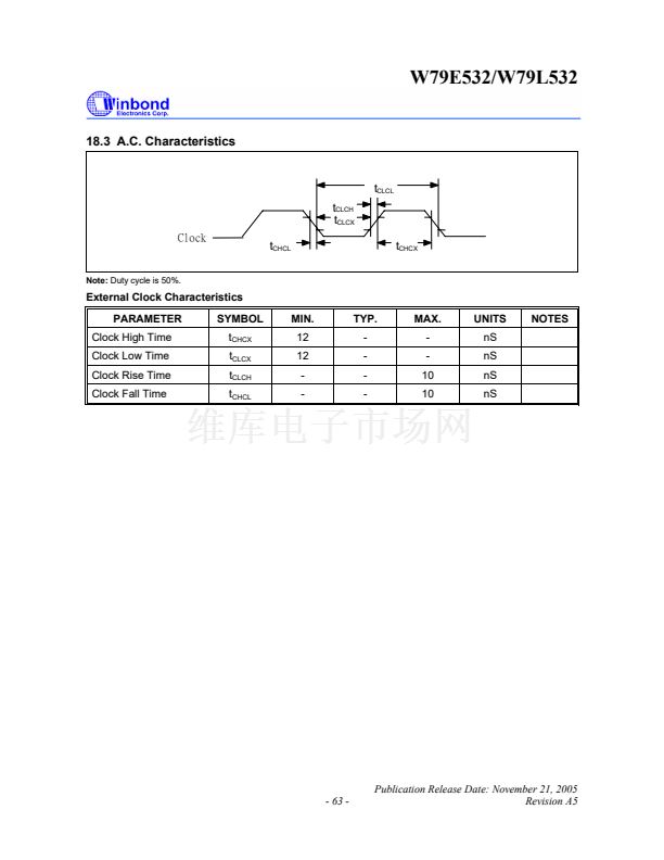
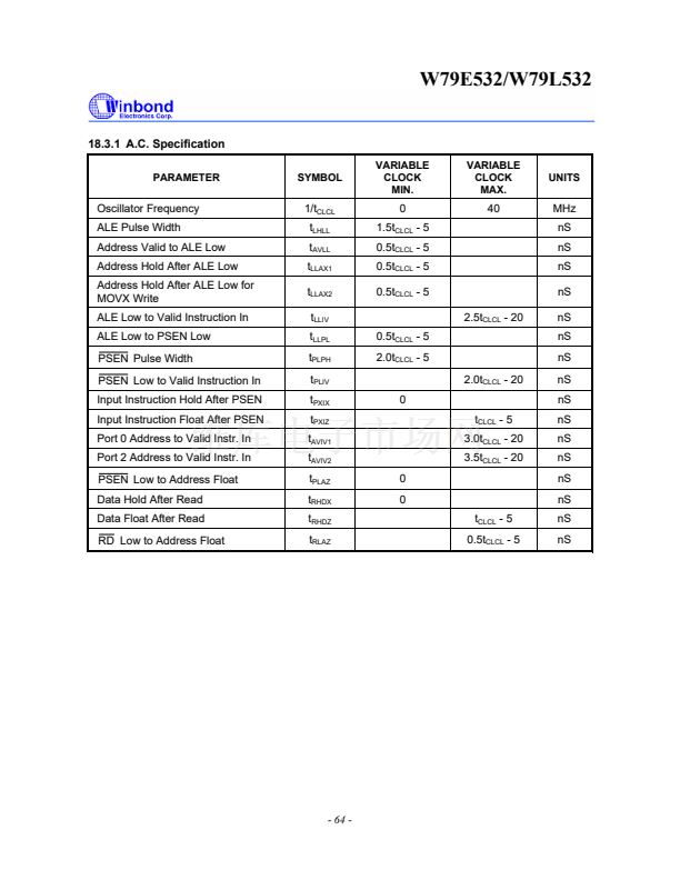
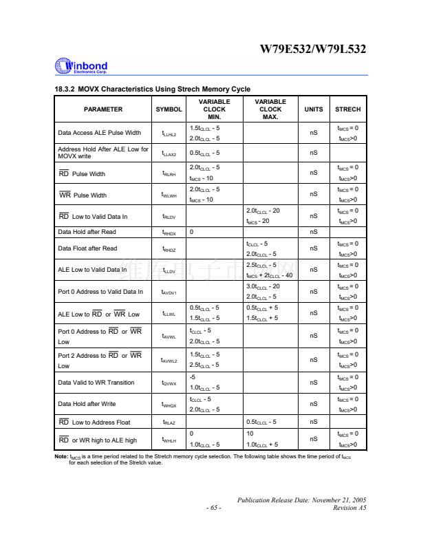
W79E532/W79L532
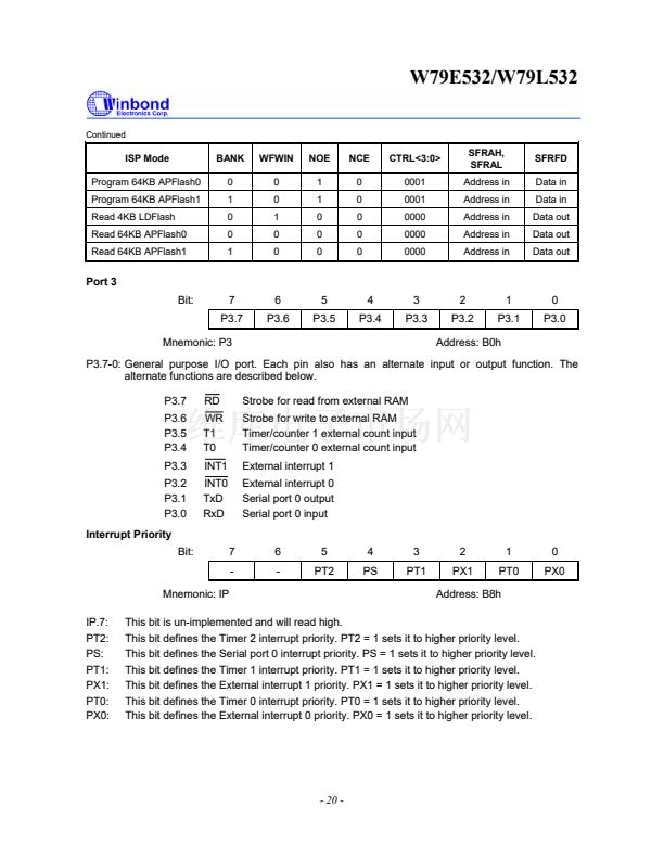
Continued
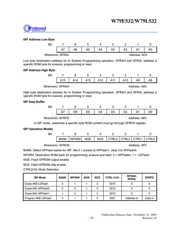
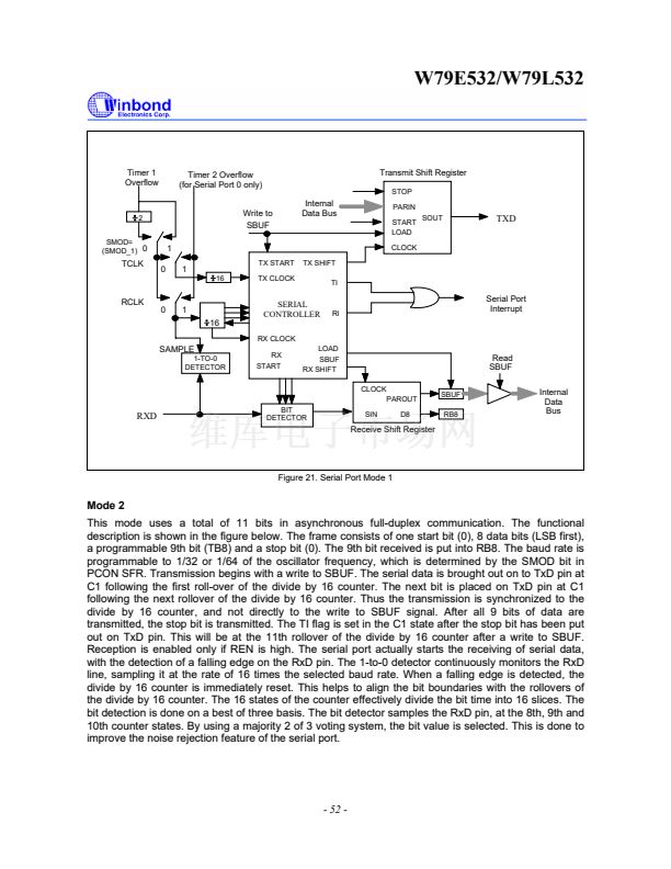
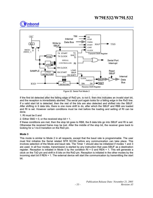
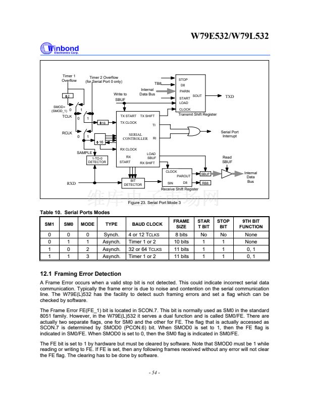
ISP Mode
Program 64KB APFlash0
Program 64KB APFlash1
Read 4KB LDFlash
Read 64KB APFlash0
Read 64KB APFlash1
BANK
0
1
0
0
1
WFWIN
0
0
1
0
0
NOE
1
1
0
0
0
NCE
0
0
0
0
0
CTRL<3:0>
0001
0001
0000
0000
0000
SFRAH,
SFRAL
Address in
Address in
Address in
Address in
Address in
SFRFD
Data in
Data in
Data out
Data out
Data out
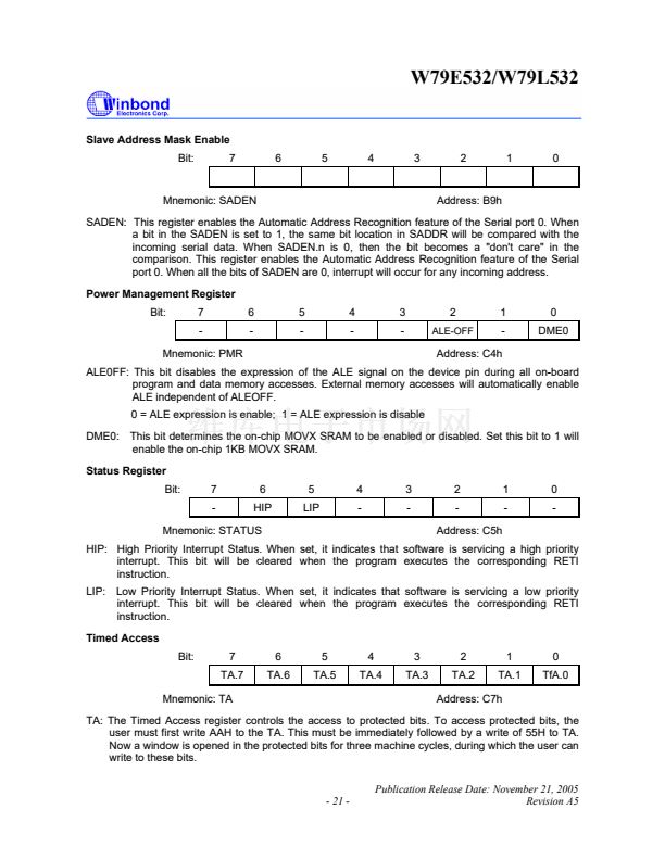
Port 3
Bit:
7
P3.7
Mnemonic: P3
6
P3.6
5
P3.5
4
P3.4
3
P3.3
2
P3.2
1
P3.1
0
P3.0
Address: B0h
P3.7-0: General purpose I/O port. Each pin also has an alternate input or output function. The
alternate functions are described below.
P3.7
P3.6
P3.5
P3.4
P3.3
P3.2
P3.1
P3.0
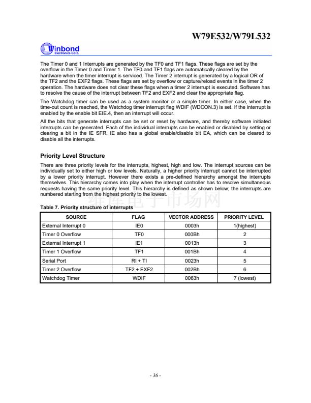
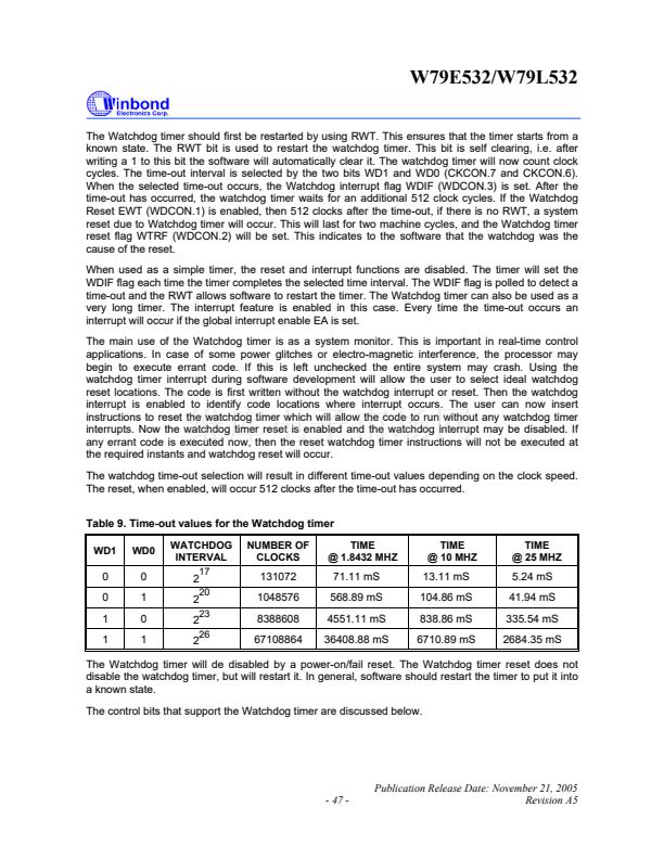
Interrupt Priority
Bit:
7
-
Mnemonic: IP
IP.7:
PT2:
PS:
PT1:
PX1:
PT0:
PX0:
6
-
5
PT2
4
PS
3
PT1
2
PX1
1
PT0
0
PX0
RD
WR
T1
T0
INT1
INT0
TxD
RxD
Strobe for read from external RAM
Strobe for write to external RAM
Timer/counter 1 external count input
Timer/counter 0 external count input
External interrupt 1
External interrupt 0
Serial port 0 output
Serial port 0 input
Address: B8h
This bit is un-implemented and will read high.
This bit defines the Timer 2 interrupt priority. PT2 = 1 sets it to higher priority level.
This bit defines the Serial port 0 interrupt priority. PS = 1 sets it to higher priority level.
This bit defines the Timer 1 interrupt priority. PT1 = 1 sets it to higher priority level.
This bit defines the External interrupt 1 priority. PX1 = 1 sets it to higher priority level.
This bit defines the Timer 0 interrupt priority. PT0 = 1 sets it to higher priority level.
This bit defines the External interrupt 0 priority. PX0 = 1 sets it to higher priority level.
- 20 -


 1
1
 2
2
 3
3
 4
4
 5
5
 6
6
 7
7
 8
8
 9
9
 10
10
 11
11
 12
12
 13
13
 14
14
 15
15
 16
16
 17
17
 18
18
 19
19
 20
20
 21
21
 22
22
 23
23
 24
24
 25
25
 26
26
 27
27
 28
28
 29
29
 30
30
 31
31
 32
32
 33
33
 34
34
 35
35
 36
36
 37
37
 38
38
 39
39
 40
40
 41
41
 42
42
 43
43
 44
44
 45
45
 46
46
 47
47
 48
48
 49
49
 50
50
 51
51
 52
52
 53
53
 54
54
 55
55
 56
56
 57
57
 58
58
 59
59
 60
60
 61
61
 62
62
 63
63
 64
64
 65
65
 66
66
 67
67
 68
68
 69
69
 70
70
 71
71
 72
72
 73
73
 74
74
 75
75
 76
76
 77
77
