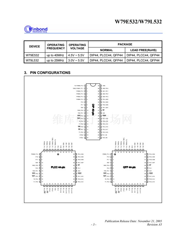
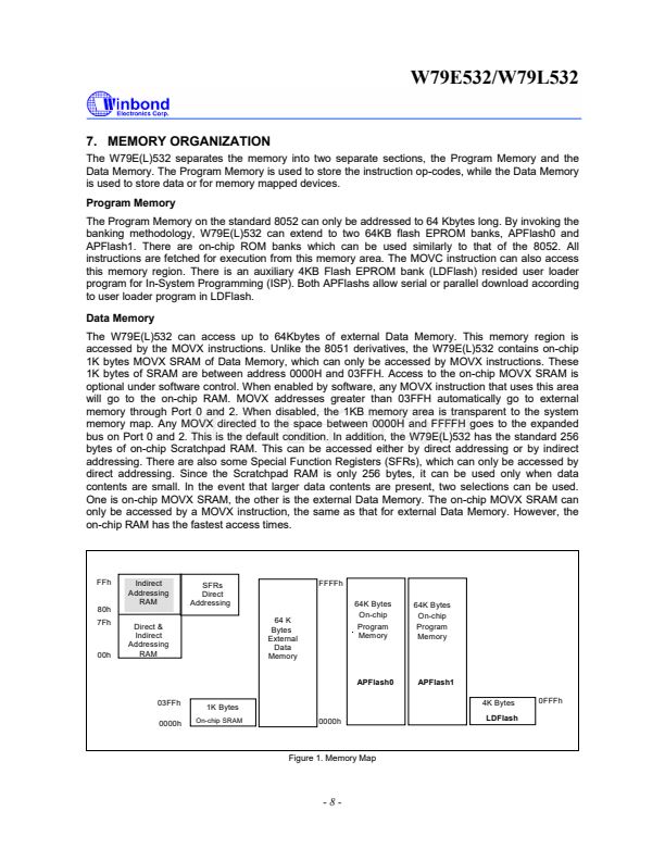
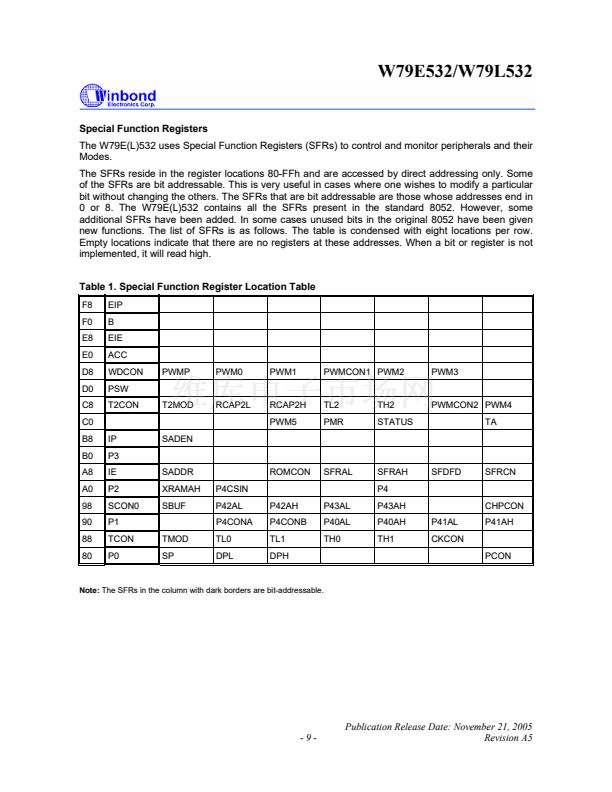
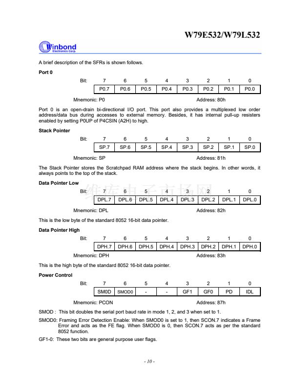
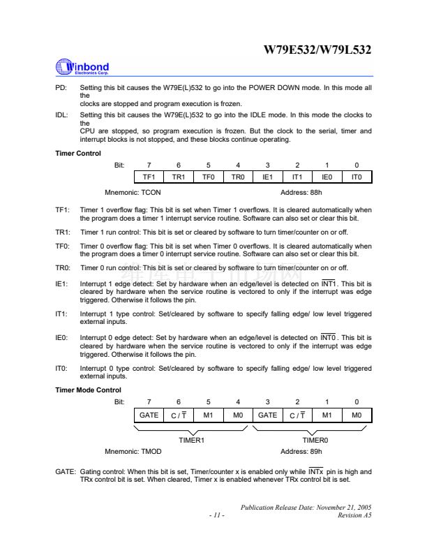
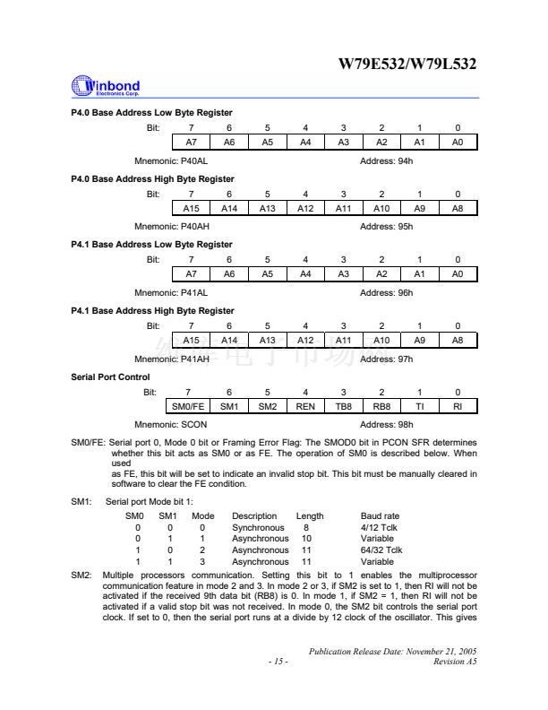
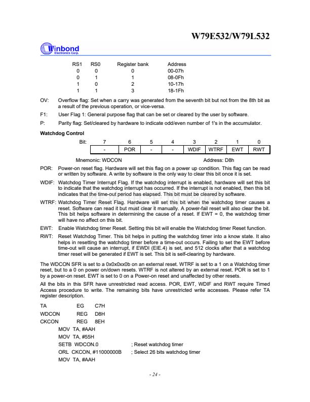
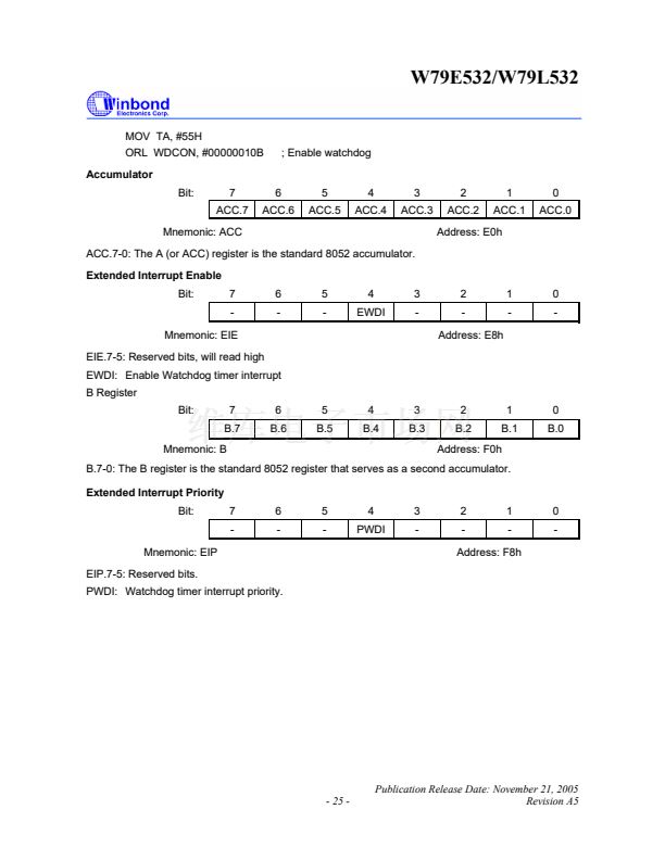
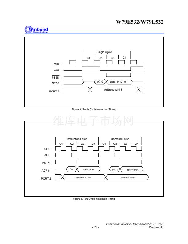
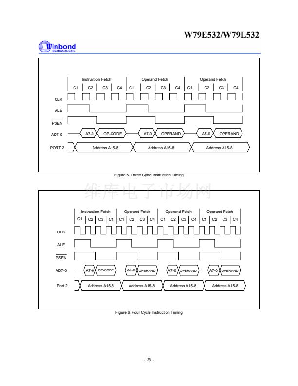
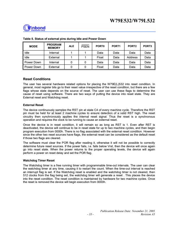
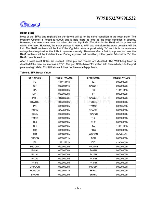
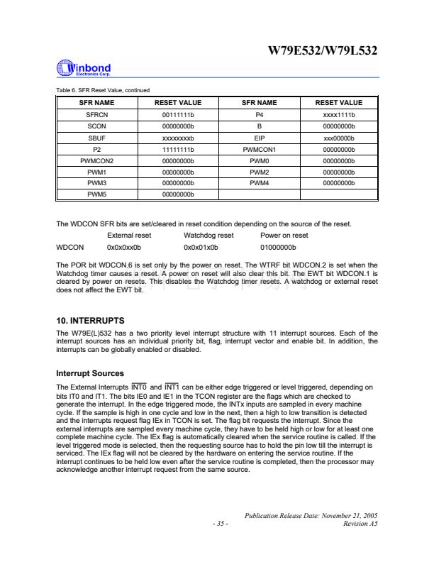
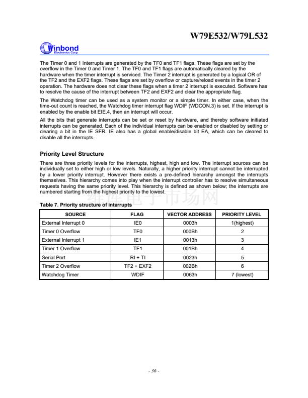
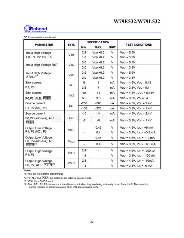
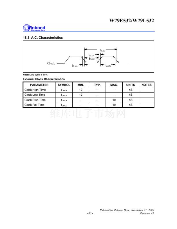
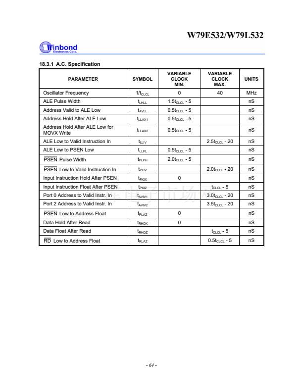
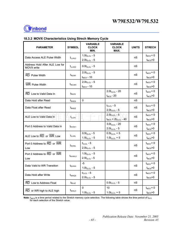
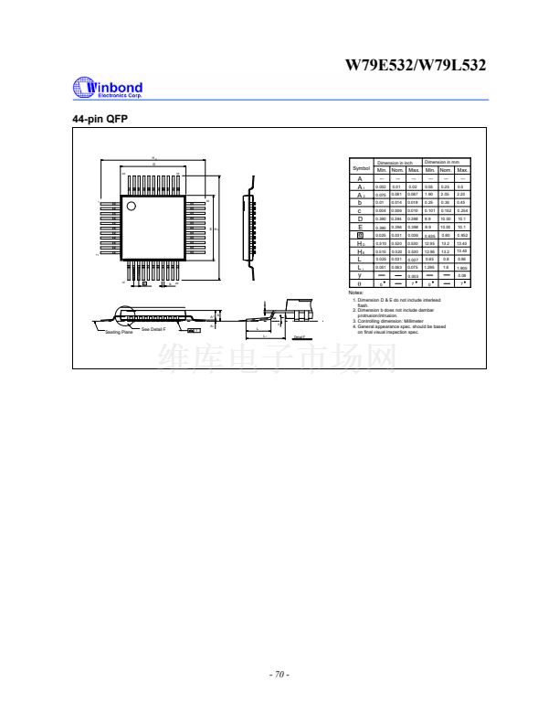
W79E532/W79L532
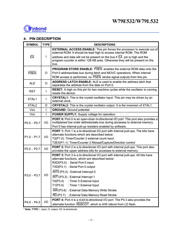
4. PIN DESCRIPTION
SYMBOL
TYPE
DESCRIPTIONS
EA
I
EXTERNAL ACCESS ENABLE:
This pin forces the processor to execute out of
external ROM. It should be kept high to access internal ROM. The ROM
address and data will not be present on the bus if
EA
pin is high and the
program counter is within 128 KB area. Otherwise they will be present on the
bus.
PROGRAM STORE ENABLE:
PSEN
enables the external ROM data onto the
Port 0 address/data bus during fetch and MOVC operations. When internal
ROM access is performed, no
PSEN
strobe signal outputs from this pin.
ADDRESS LATCH ENABLE:
ALE is used to enable the address latch that
separates the address from the data on Port 0.
RESET:
A high on this pin for two machine cycles while the oscillator is running
resets the device.
CRYSTAL1:
This is the crystal oscillator input. This pin may be driven by an
external clock.
CRYSTAL2:
This is the crystal oscillator output. It is the inversion of XTAL1.
GROUND:
Ground potential
POWER SUPPLY:
Supply voltage for operation.
PORT 0:
Port 0 is an open-drain bi-directional I/O port. This port also provides a
multiplexed low order address/data bus during accesses to external memory.
Port 0 has internal pull-up resisters enabled by software.
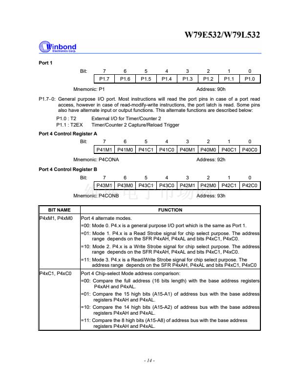
PORT 1:
Port 1 is a bi-directional I/O port with internal pull-ups. The bits have
alternate functions which are described below:
T2(P1.0): Timer/Counter 2 external count input
T2EX(P1.1): Timer/Counter 2 Reload/Capture/Direction control
PORT 2:
Port 2 is a bi-directional I/O port with internal pull-ups. This port also
provides the upper address bits for accesses to external memory.
PORT 3:
Port 3 is a bi-directional I/O port with internal pull-ups. All bits have
alternate functions, which are described below:
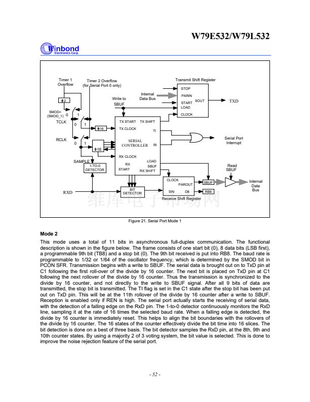
RXD(P3.0) : Serial Port 0 input
TXD(P3.1) : Serial Port 0 output
PSEN
O
ALE
RST
XTAL1
XTAL2
V
SS
V
DD
P0.0
鈭?/div>
P0.7
O
I
I
O
I
I
I/O
P1.0
鈭?/div>
P1.7
I/O
P2.0
鈭?/div>
P2.7
I/O
P3.0
鈭?/div>
P3.7
INT0
(P3.2) : External Interrupt 0
I/O
INT1
(P3.3) : External Interrupt 1
T0(P3.4) : Timer 0 External Input
T1(P3.5) : Timer 1 External Input
WR
(P3.6) : External Data Memory Write Strobe
RD
(P3.7) : External Data Memory Read Strobe
P4.0
鈭?/div>
P4.3
I/O
PORT 4:
Port 4 is a 4-bit bi-directional I/O port. The P4.3 also provides the
alternate function
REBOOT
which is H/W reboot from LD flash.
* Note: TYPE
I : input, O: output, I/O: bi-directional.
-4-
W79E532A40DL 产品属性
10
集成电路 (IC)
嵌入式 - 微控制器,
W79
8052
8-位
40MHz
EBI/EMI,串行端口
POR,PWM,WDT
32
128KB(128K x 8)
闪存
-
1.25K x 8
3 V ~ 5.5 V
-
内部
0°C ~ 70°C
40-DIP
管件


 1
1
 2
2
 3
3
 4
4
 5
5
 6
6
 7
7
 8
8
 9
9
 10
10
 11
11
 12
12
 13
13
 14
14
 15
15
 16
16
 17
17
 18
18
 19
19
 20
20
 21
21
 22
22
 23
23
 24
24
 25
25
 26
26
 27
27
 28
28
 29
29
 30
30
 31
31
 32
32
 33
33
 34
34
 35
35
 36
36
 37
37
 38
38
 39
39
 40
40
 41
41
 42
42
 43
43
 44
44
 45
45
 46
46
 47
47
 48
48
 49
49
 50
50
 51
51
 52
52
 53
53
 54
54
 55
55
 56
56
 57
57
 58
58
 59
59
 60
60
 61
61
 62
62
 63
63
 64
64
 65
65
 66
66
 67
67
 68
68
 69
69
 70
70
 71
71
 72
72
 73
73
 74
74
 75
75
 76
76
 77
77
