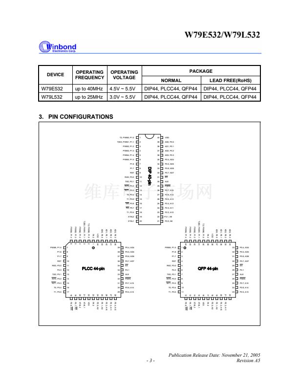
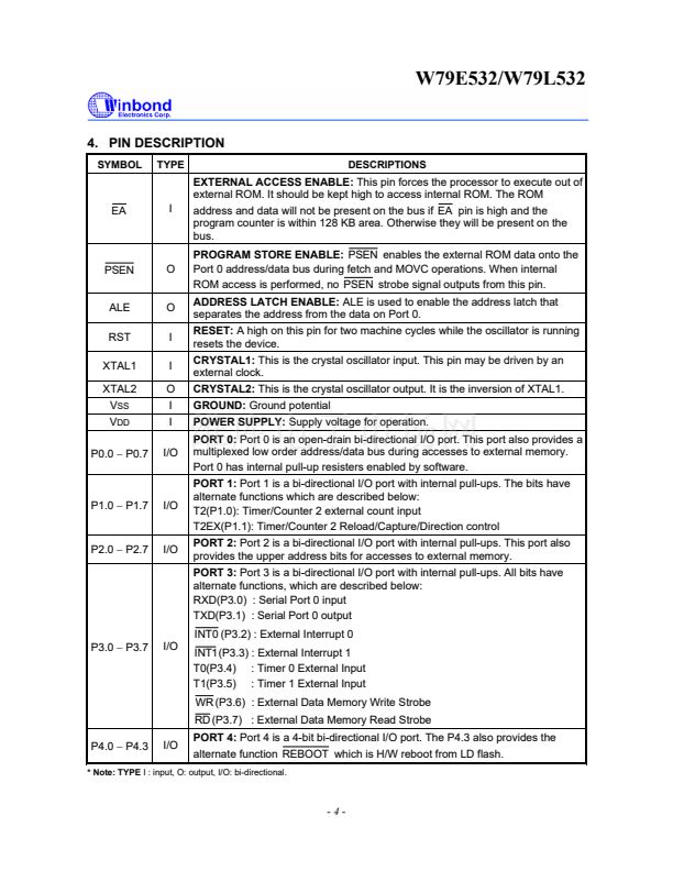
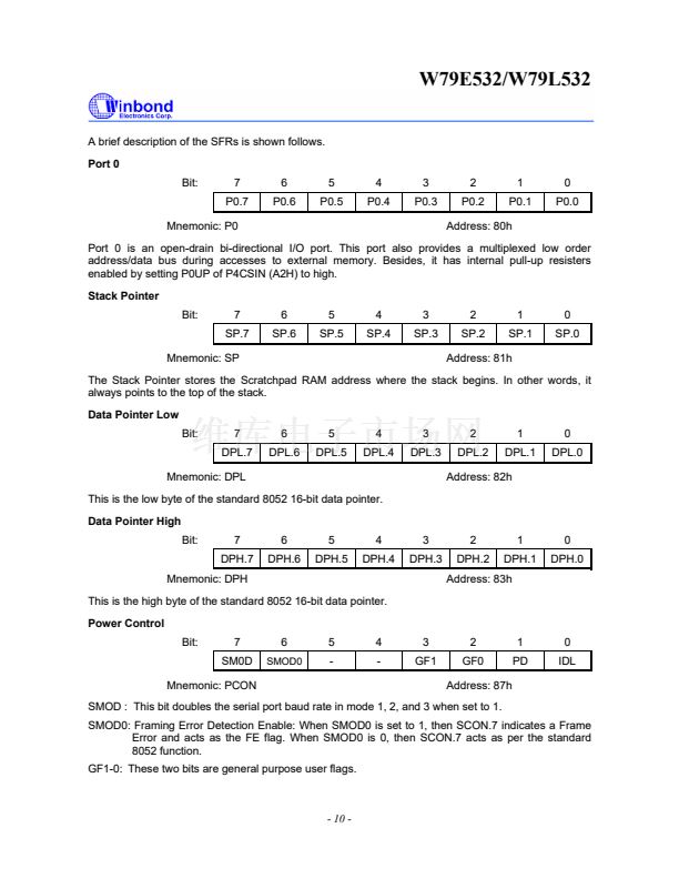
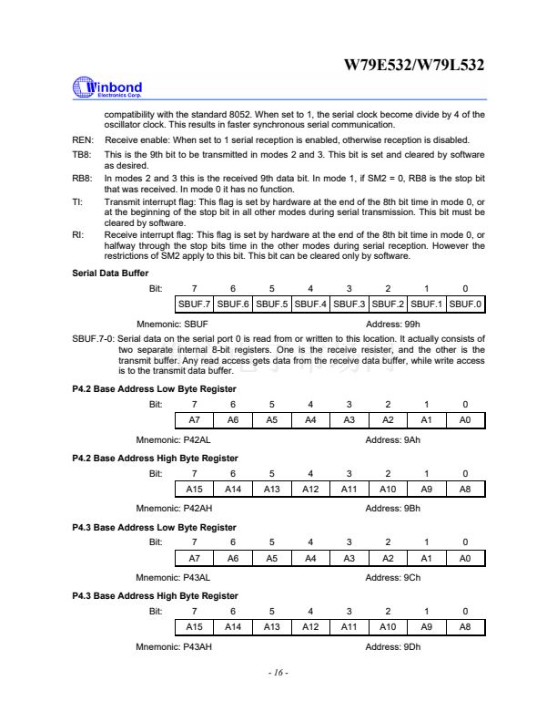
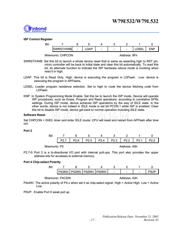
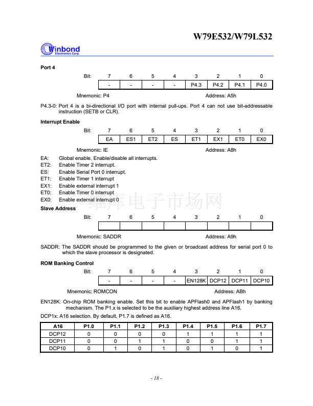
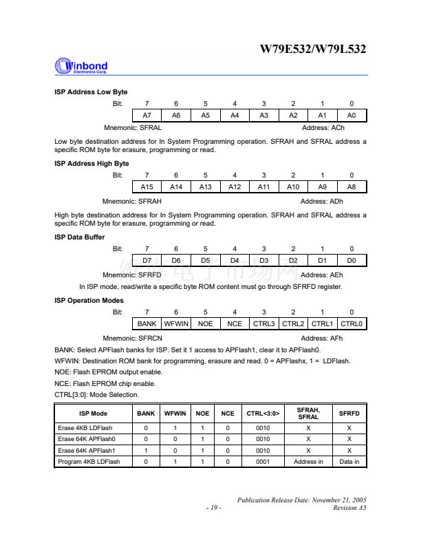
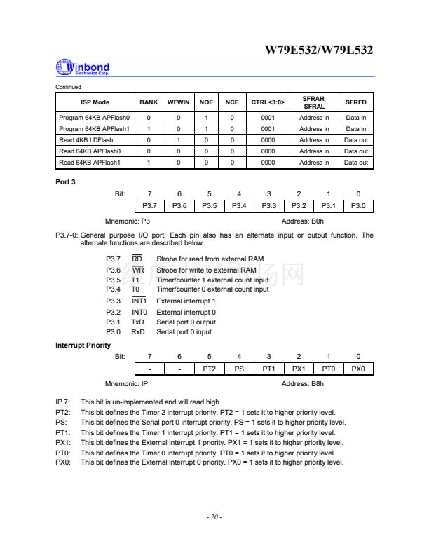
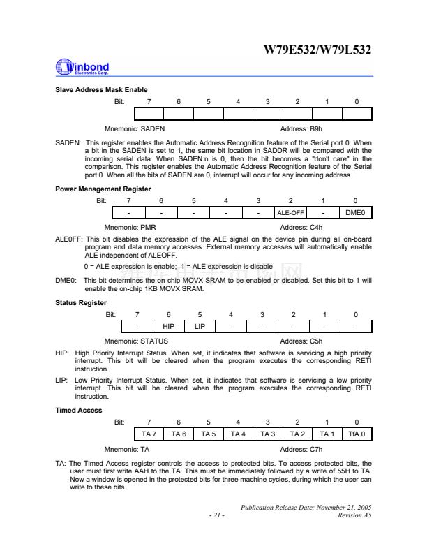
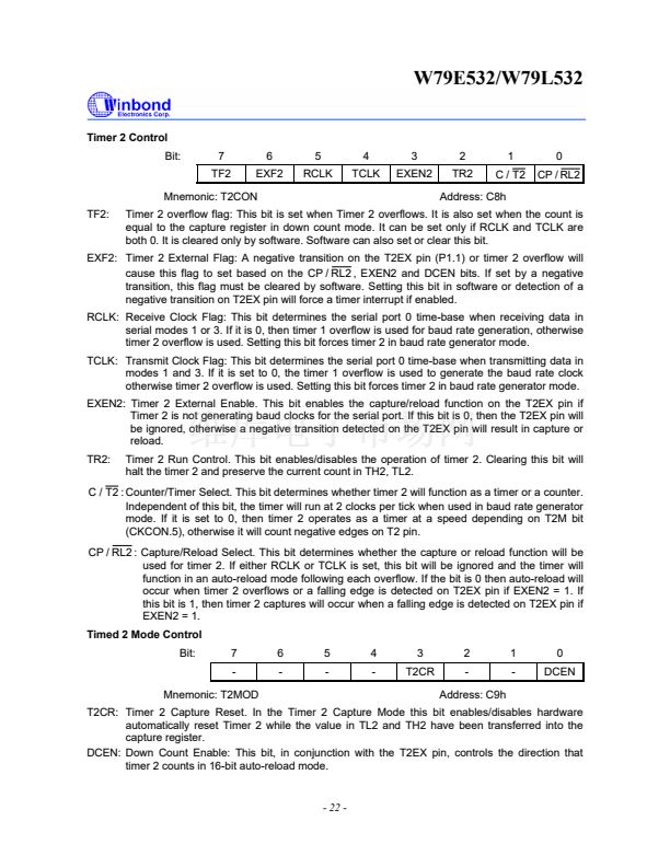
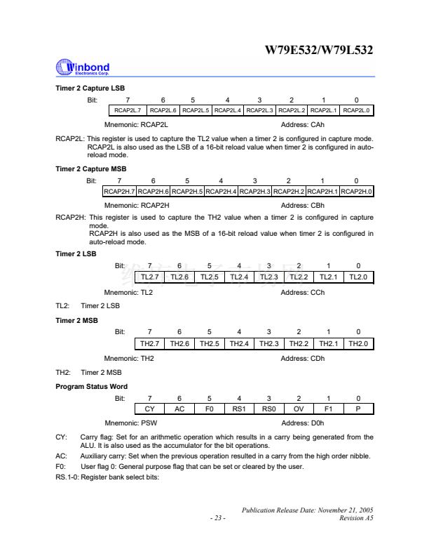
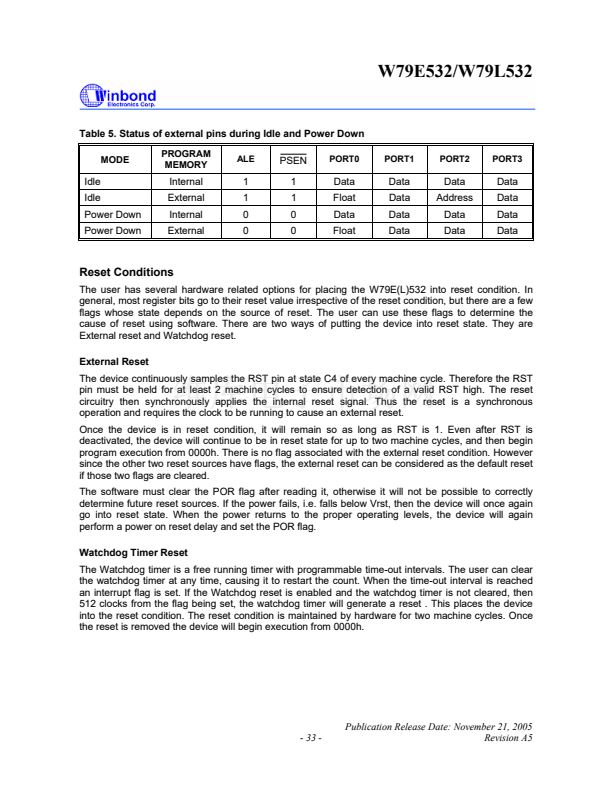
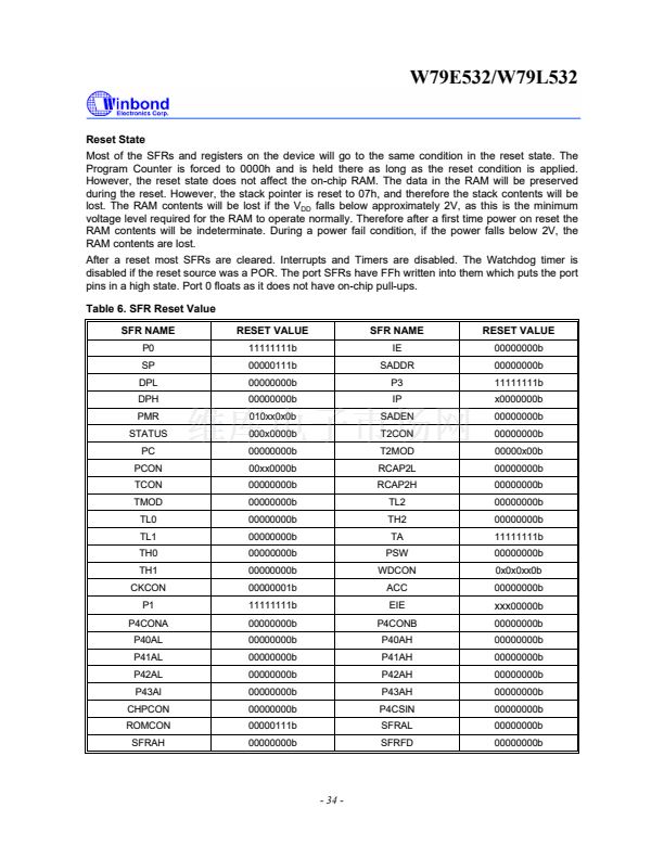
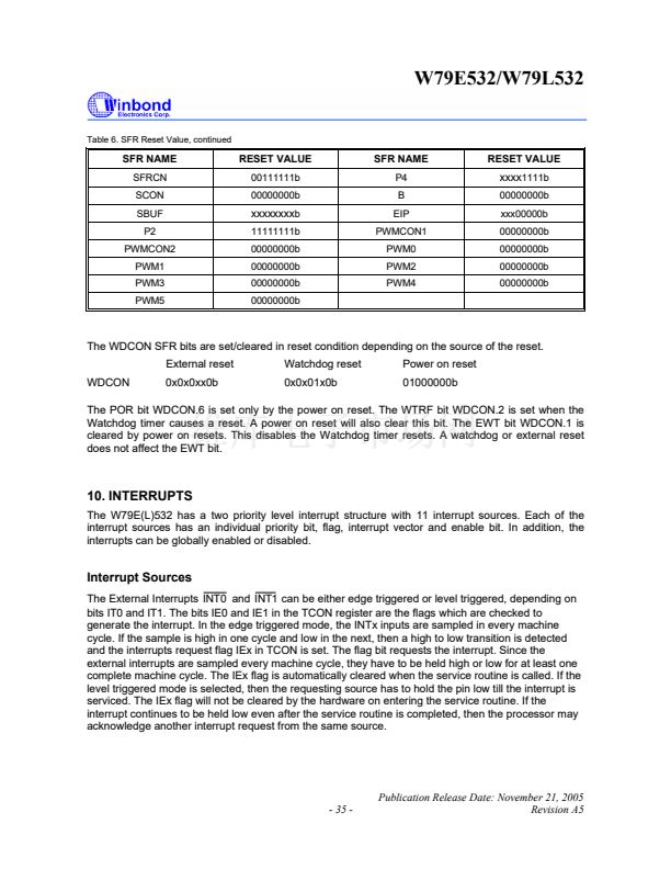
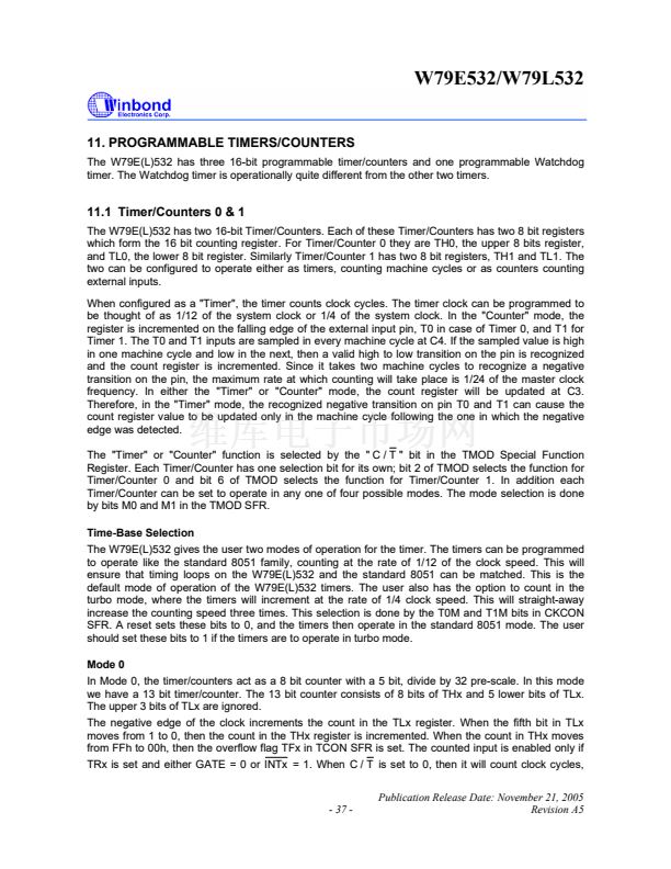
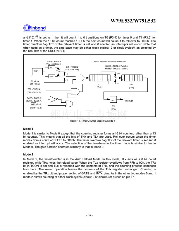
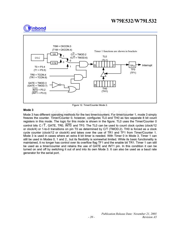
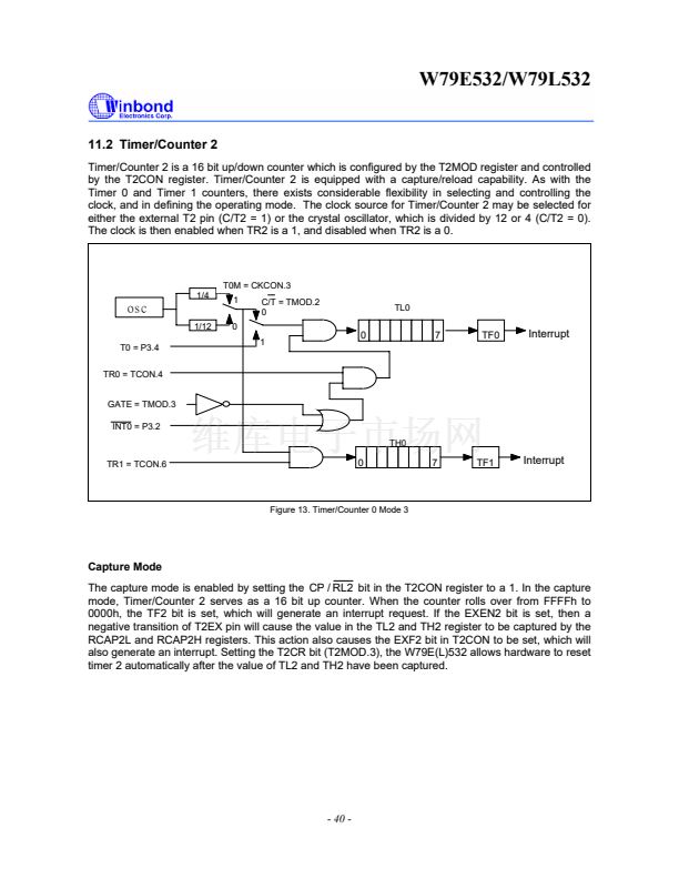
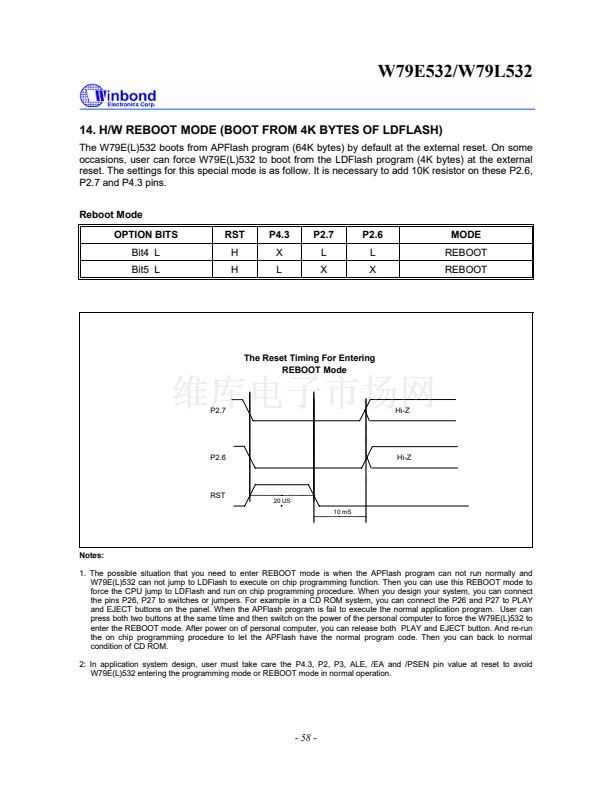
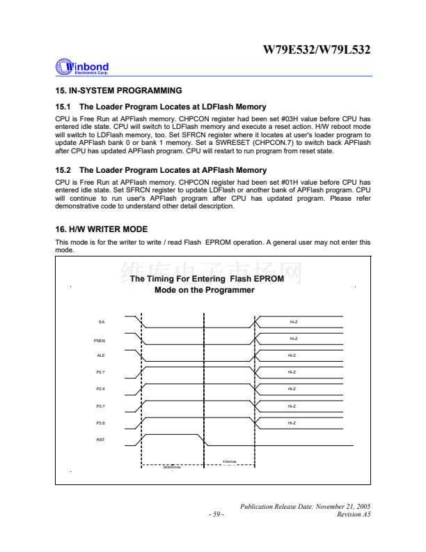
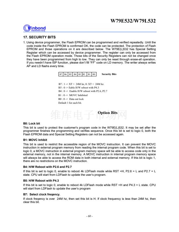
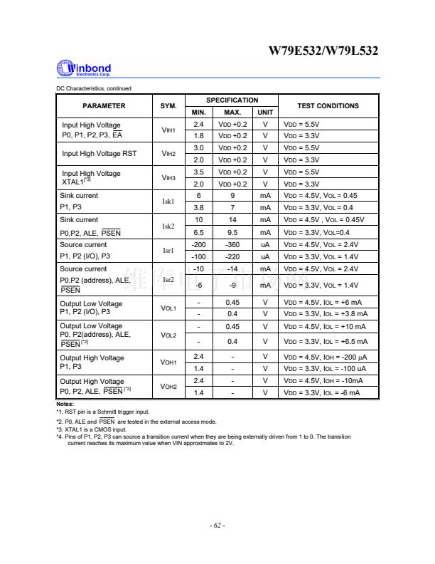
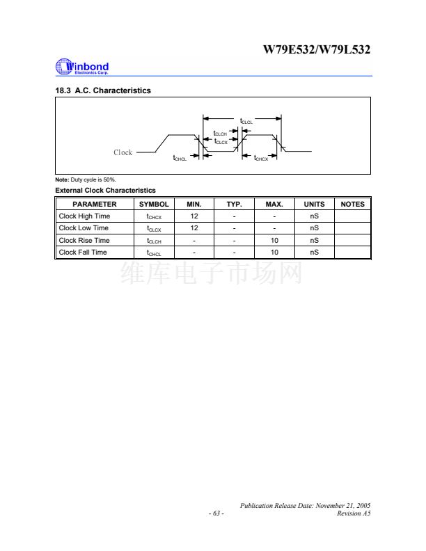
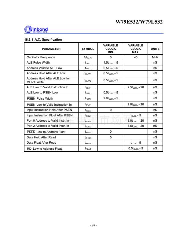
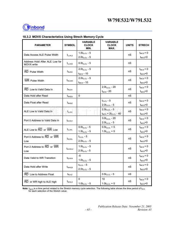
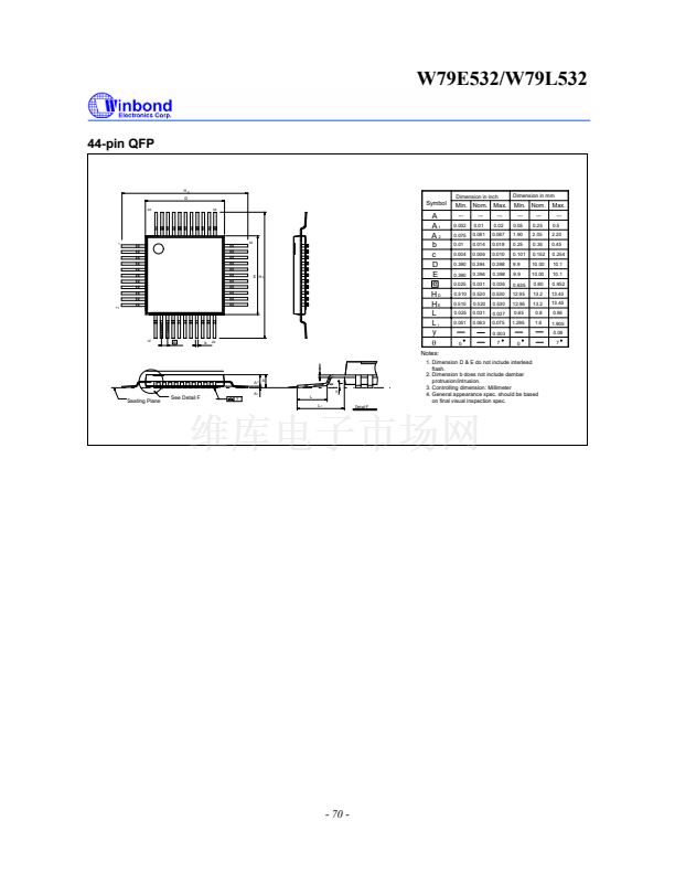
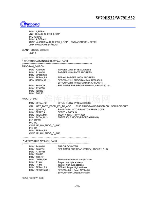
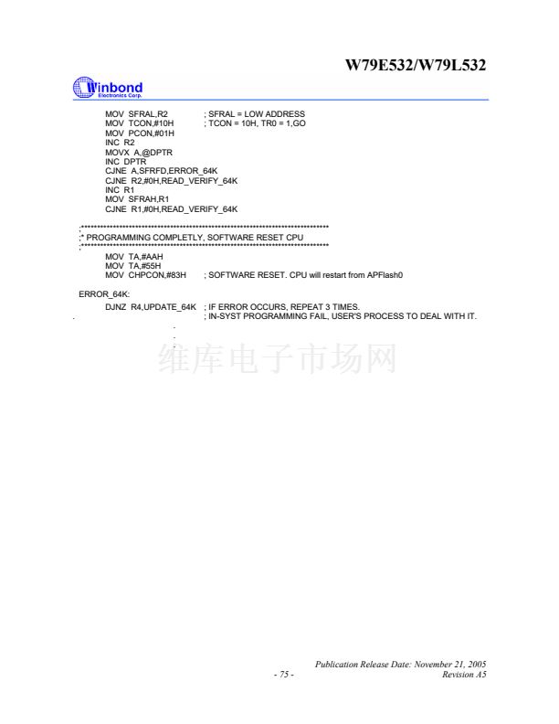
W79E532/W79L532
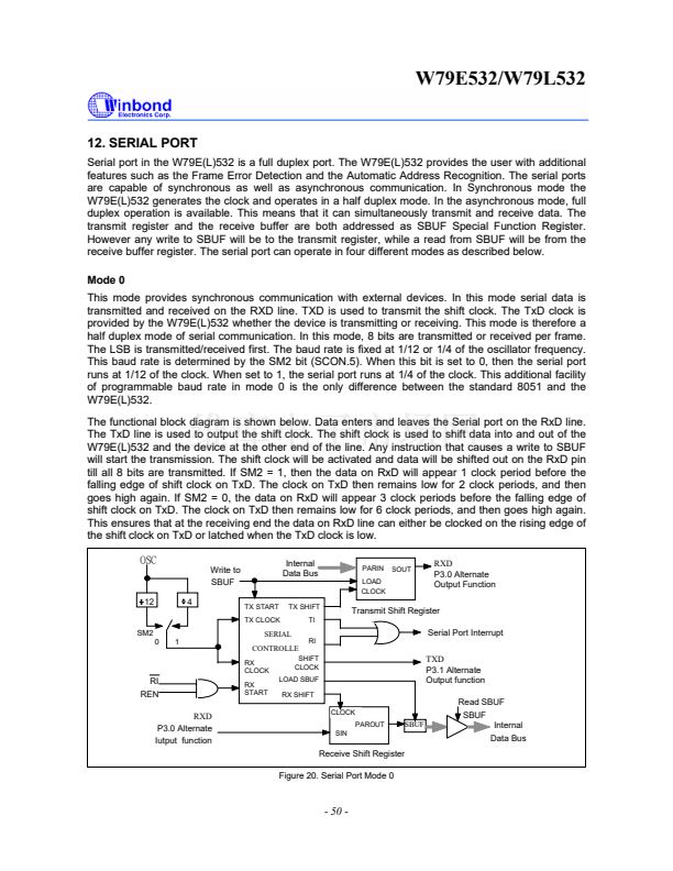
12. SERIAL PORT
Serial port in the W79E(L)532 is a full duplex port. The W79E(L)532 provides the user with additional
features such as the Frame Error Detection and the Automatic Address Recognition. The serial ports
are capable of synchronous as well as asynchronous communication. In Synchronous mode the
W79E(L)532 generates the clock and operates in a half duplex mode. In the asynchronous mode, full
duplex operation is available. This means that it can simultaneously transmit and receive data. The
transmit register and the receive buffer are both addressed as SBUF Special Function Register.
However any write to SBUF will be to the transmit register, while a read from SBUF will be from the
receive buffer register. The serial port can operate in four different modes as described below.
Mode 0
This mode provides synchronous communication with external devices. In this mode serial data is
transmitted and received on the RXD line. TXD is used to transmit the shift clock. The TxD clock is
provided by the W79E(L)532 whether the device is transmitting or receiving. This mode is therefore a
half duplex mode of serial communication. In this mode, 8 bits are transmitted or received per frame.
The LSB is transmitted/received first. The baud rate is fixed at 1/12 or 1/4 of the oscillator frequency.
This baud rate is determined by the SM2 bit (SCON.5). When this bit is set to 0, then the serial port
runs at 1/12 of the clock. When set to 1, the serial port runs at 1/4 of the clock. This additional facility
of programmable baud rate in mode 0 is the only difference between the standard 8051 and the
W79E(L)532.
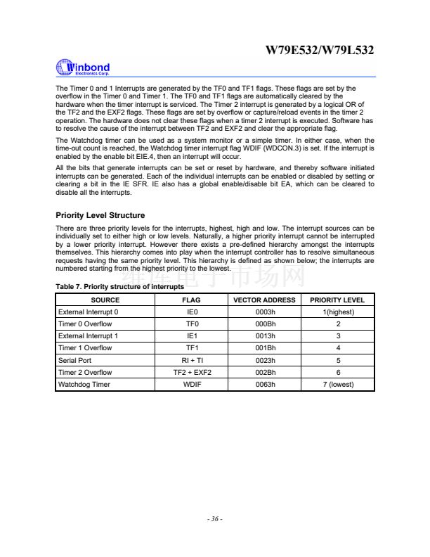
The functional block diagram is shown below. Data enters and leaves the Serial port on the RxD line.
The TxD line is used to output the shift clock. The shift clock is used to shift data into and out of the
W79E(L)532 and the device at the other end of the line. Any instruction that causes a write to SBUF
will start the transmission. The shift clock will be activated and data will be shifted out on the RxD pin
till all 8 bits are transmitted. If SM2 = 1, then the data on RxD will appear 1 clock period before the
falling edge of shift clock on TxD. The clock on TxD then remains low for 2 clock periods, and then
goes high again. If SM2 = 0, the data on RxD will appear 3 clock periods before the falling edge of
shift clock on TxD. The clock on TxD then remains low for 6 clock periods, and then goes high again.
This ensures that at the receiving end the data on RxD line can either be clocked on the rising edge of
the shift clock on TxD or latched when the TxD clock is low.
OSC
Write to
SBUF
12
4
TX START
TX CLOCK
Internal
Data Bus
PARIN
LOAD
CLOCK
SOUT
RXD
P3.0 Alternate
Output Function
TX SHIFT
TI
Transmit Shift Register
Serial Port Interrupt
SM2
0
1
SERIAL
CONTROLLE
RX
CLOCK
RI
SHIFT
CLOCK
RI
REN
RXD
P3.0 Alternate
Iutput function
RX
START
LOAD SBUF
RX SHIFT
CLOCK
PAROUT
SIN
TXD
P3.1 Alternate
Output function
Read SBUF
SBUF
Internal
Data Bus
SBUF
Receive Shift Register
Figure 20. Serial Port Mode 0
- 50 -


 1
1
 2
2
 3
3
 4
4
 5
5
 6
6
 7
7
 8
8
 9
9
 10
10
 11
11
 12
12
 13
13
 14
14
 15
15
 16
16
 17
17
 18
18
 19
19
 20
20
 21
21
 22
22
 23
23
 24
24
 25
25
 26
26
 27
27
 28
28
 29
29
 30
30
 31
31
 32
32
 33
33
 34
34
 35
35
 36
36
 37
37
 38
38
 39
39
 40
40
 41
41
 42
42
 43
43
 44
44
 45
45
 46
46
 47
47
 48
48
 49
49
 50
50
 51
51
 52
52
 53
53
 54
54
 55
55
 56
56
 57
57
 58
58
 59
59
 60
60
 61
61
 62
62
 63
63
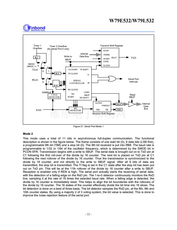
 64
64
 65
65
 66
66
 67
67
 68
68
 69
69
 70
70
 71
71
 72
72
 73
73
 74
74
 75
75
 76
76
 77
77
