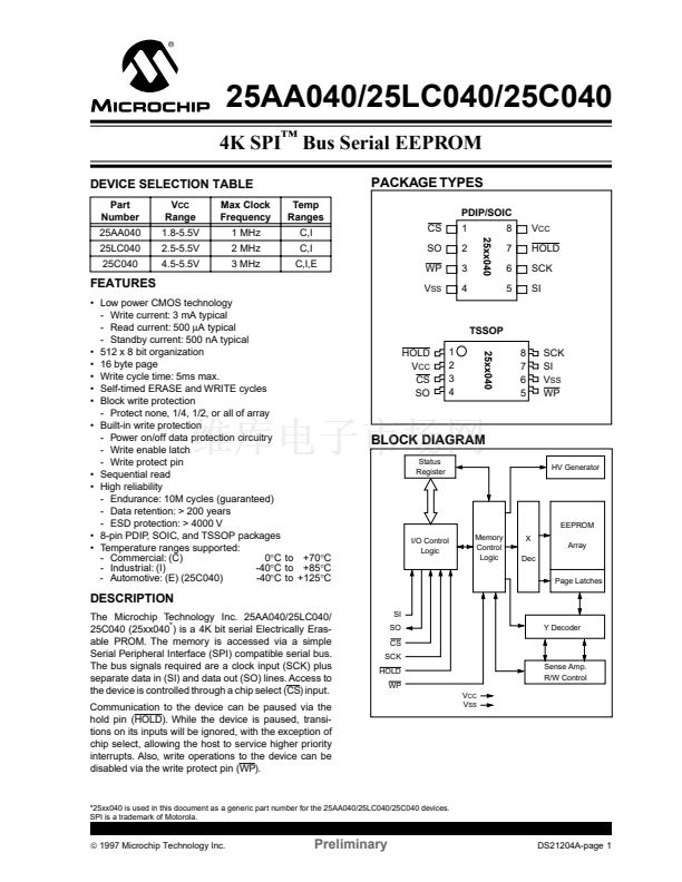
25AA040/25LC040/25C040
3.7
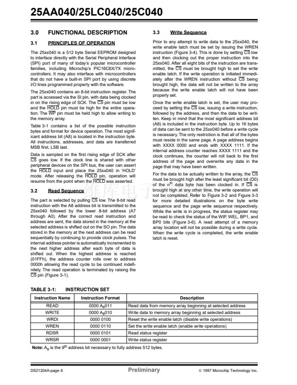
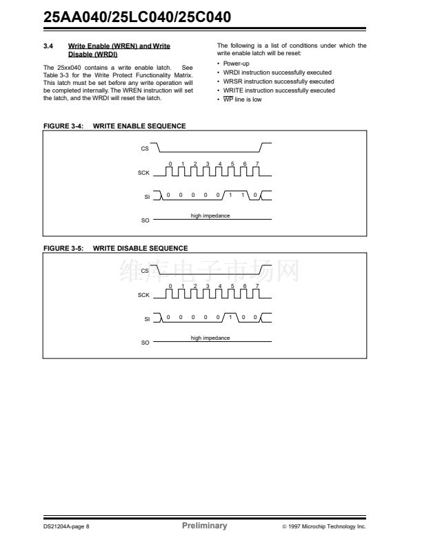
Data Protection
3.8
Power On State
The following protection has been implemented to pre-
vent inadvertent writes to the array:
鈥?The write enable latch is reset on power-up.
鈥?A write enable instruction must be issued to set
the write enable latch.
鈥?After a byte write, page write, or status register
write, the write enable latch is reset.
鈥?CS must be set high after the proper number of
clock cycles to start an internal write cycle.
鈥?Access to the array during an internal write cycle
is ignored and programming is continued.
鈥?The write enable latch is reset when the WP pin is
low.
The 25xx040 powers on in the following state:
鈥?/div>
鈥?/div>
鈥?/div>
鈥?/div>
The device is in low power standby mode (CS= 1).
The write enable latch is reset.
SO is in high impedance state.
A low level on CS is required to enter active state.
.
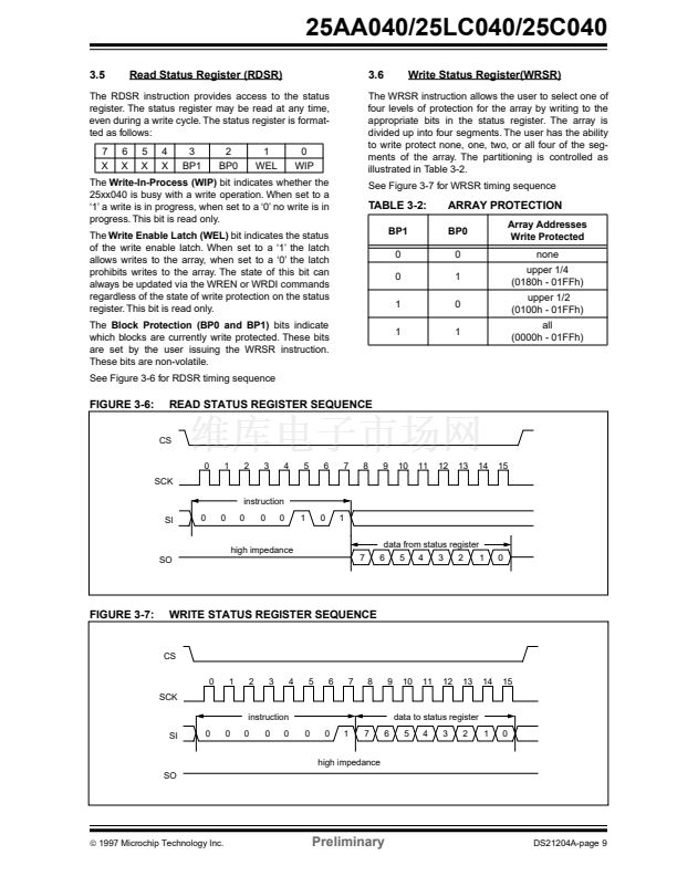
TABLE 3-3:
WP
Low
High
High
WRITE PROTECT FUNCTIONALITY MATRIX
WEL
X
0
1
Protected Blocks
Protected
Protected
Protected
Unprotected Blocks
Protected
Protected
Writable
Status Register
Protected
Protected
Writable
DS21204A-page 10
Preliminary
漏
1997 Microchip Technology Inc.


 1
1
 2
2
 3
3
 4
4
 5
5
 6
6
 7
7
 8
8
 9
9
 10
10
 11
11
 12
12
