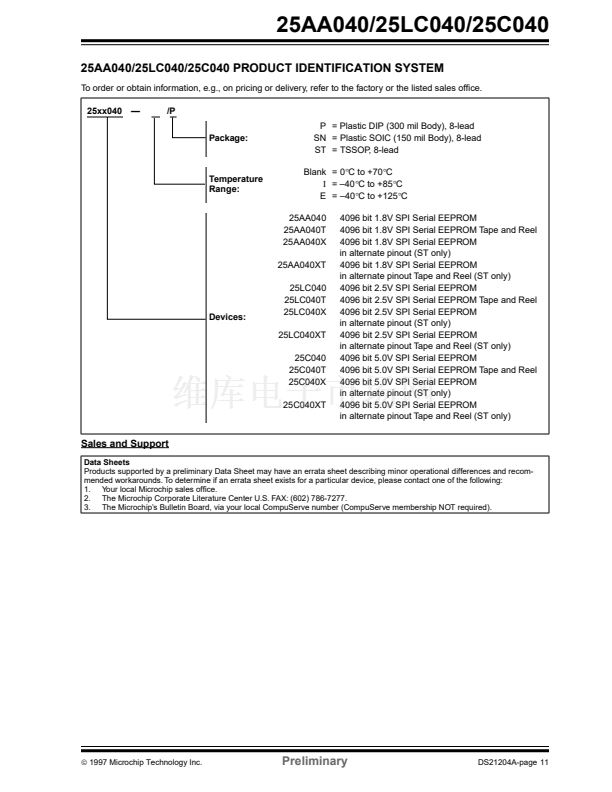
25AA040/25LC040/25C040
2.0
2.1
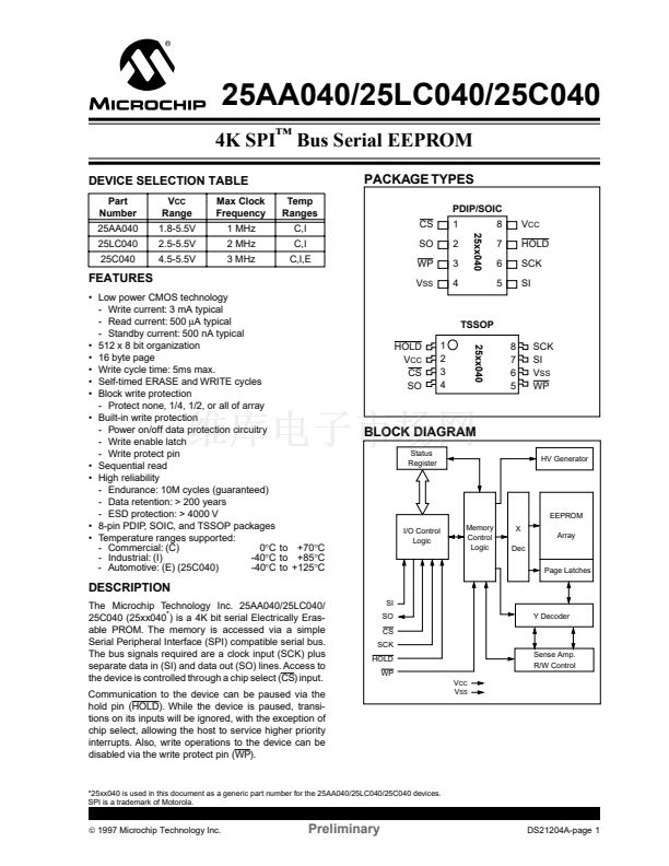
PIN DESCRIPTIONS
Chip Select (CS)
2.5
Write Protect (WP)
A low level on this pin selects the device. A high level
deselects the device and forces it into standby mode.
However, a programming cycle which is already initi-
ated or in progress will be completed, regardless of the
CS input signal. If CS is brought high during a program
cycle, the device will go in standby mode as soon as
the programming cycle is complete. As soon as the
device is deselected, SO goes to the high impedance
state, allowing multiple parts to share the same SPI
bus. A low to high transition on CS after a valid write
sequence initiates an internal write cycle. After power-
up, a low level on CS is required prior to any sequence
being initiated.
This pin is a hardware write protect input pin. When
WP is low, all writes to the array or status register are
disabled, but any other operation functions normally.
When WP is high, all functions, including non-volatile
writes operate normally. WP going low at any time will
reset the write enable latch and inhibit programming,
except when an internal write has already begun. If an
internal write cycle has already begun, WP going low
will have no effect on the write. See Table 3-2 for Write
Protect Functionality Matrix.
2.6
Hold (HOLD)
2.2
Serial Input (SI)
The SI pin is used to transfer data into the device. It
receives instructions, addresses, and data. Data is
latched on the rising edge of the serial clock.
2.3
Serial Output (SO)
The SO pin is used to transfer data out of the 25xx040.
During a read cycle, data is shifted out on this pin after
the falling edge of the serial clock.
2.4
Serial Clock (SCK)
The SCK is used to synchronize the communication
between a master and the 25xx040. Instructions,
addresses, or data present on the SI pin are latched
on the rising edge of the clock input, while data on the
SO pin is updated after the falling edge of the clock
input.
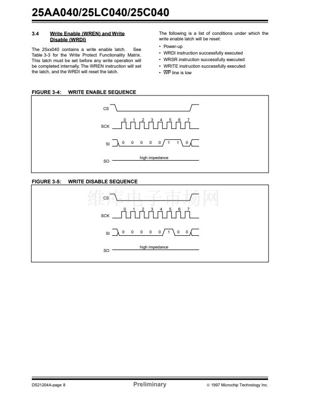
The HOLD pin is used to suspend transmission to the
25xx040 while in the middle of a serial sequence with-
out having to re-transmit the entire sequence over at a
later time. It must be held high any time this function is
not being used. Once the device is selected and a
serial sequence is underway, the HOLD pin may be
pulled low to pause further serial communication with-
out resetting the serial sequence. The HOLD pin must
be brought low while SCK is low, otherwise the HOLD
function will not be invoked until the next SCK high to
low transition. The 25xx040 must remain selected dur-
ing this sequence. The SI, SCK, and SO pins are in a
high impedance state during the time the part is
paused and transitions on these pins will be ignored.
To resume serial communication, HOLD must be
brought high while the SCK pin is low, otherwise serial
communication will not resume. Lowering the HOLD
line at any time will tri-state the SO line.
漏
1997 Microchip Technology Inc.
Preliminary
DS21204A-page 5


 1
1
 2
2
 3
3
 4
4
 5
5
 6
6
 7
7
 8
8
 9
9
 10
10
 11
11
 12
12
