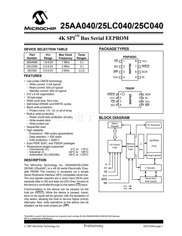
controllers. It may also interface with microcontrollers
I/O lines programmed properly with the software.
The 25xx040 contains an 8-bit instruction register. The
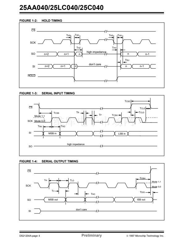
in on the rising edge of SCK. The CS pin must be low
tion. The WP pin must be held high to allow writing to
the memory array.
bytes and format for device operation. The most signif-
icant address bit (A8) is located in the instruction byte.
MSB 铿乺st, LSB last.
CS goes low. If the clock line is shared with other
the HOLD input and place the 25xx040 in 鈥楬OLD鈥?/div>
mode. After releasing the HOLD pin, operation will
resume from the point when the HOLD was asserted.
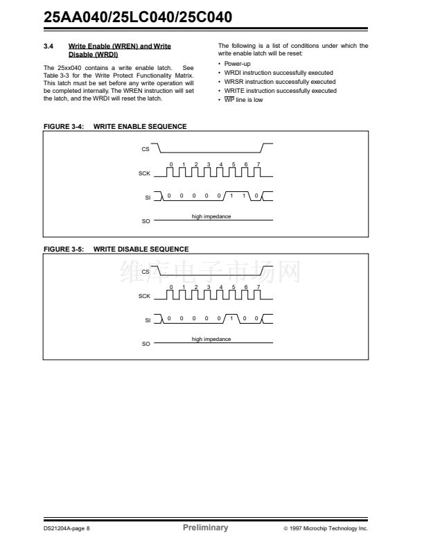
Prior to any attempt to write data to the 25xx040, the
write enable latch must be set by issuing the WREN
instruction (Figure 3-4). This is done by setting CS low
and then clocking out the proper instruction into the
25xx040. After all eight bits of the instruction are trans-
mitted, the CS must be brought high to set the write
enable latch. If the write operation is initiated immedi-
ately after the WREN instruction without CS being
brought high, the data will not be written to the array
because the write enable latch will not have been
properly set.
Once the write enable latch is set, the user may pro-
ceed by setting the CS low, issuing a write instruction,
followed by the address, and then the data to be writ-
ten. Keep in mind that the most signi铿乧ant address bit
(A8) is included in the instruction byte. Up to 16 bytes
of data can be sent to the 25xx040 before a write cycle
is necessary. The only restriction is that all of the bytes
must reside in the same page. A page address begins
with XXXX 0000 and ends with XXXX 1111. If the
internal address counter reaches XXXX 1111 and the
clock continues, the counter will roll back to the 铿乺st
address of the page and overwrite any data in the
page that may have been written.
For the data to be actually written to the array, the CS
must be brought high after the least signi铿乧ant bit (D0)
of the n
th
data byte has been clocked in. If CS is
brought high at any other time, the write operation will
not be completed. Refer to Figure 3-2 and Figure 3-3
for more detailed illustrations on the byte write
sequence and the page write sequence respectively.
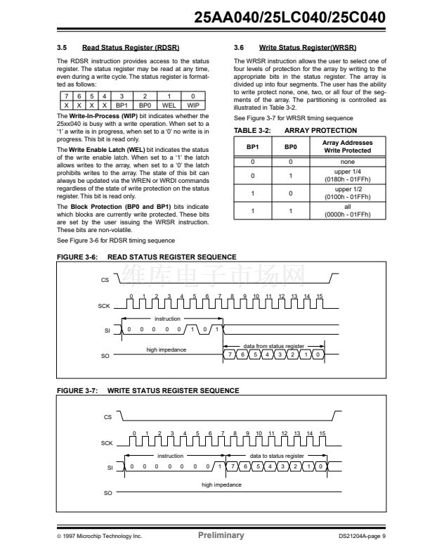
While the write is in progress, the status register may
be read to check the status of the WIP, WEL, BP1, and
BP0 bits (Figure 3-6). A read attempt of a memory
array location will not be possible during a write cycle.
When the write cycle is completed, the write enable
latch is reset.
3.2
Read Sequence
The part is selected by pulling CS low. The 8-bit read
instruction with the A8 address bit is transmitted to the
25xx040 followed by the lower 8-bit address (A7
through A0). After the correct read instruction and
address are sent, the data stored in the memory at the
selected address is shifted out on the SO pin. The data
stored in the memory at the next address can be read
sequentially by continuing to provide clock pulses. The
internal address pointer is automatically incremented to
the next higher address after each byte of data is
shifted out. When the highest address is reached
(01FFh), the address counter rolls over to address
0000h allowing the read cycle to be continued inde铿?
nitely. The read operation is terminated by raising the
CS pin (Figure 3-1).
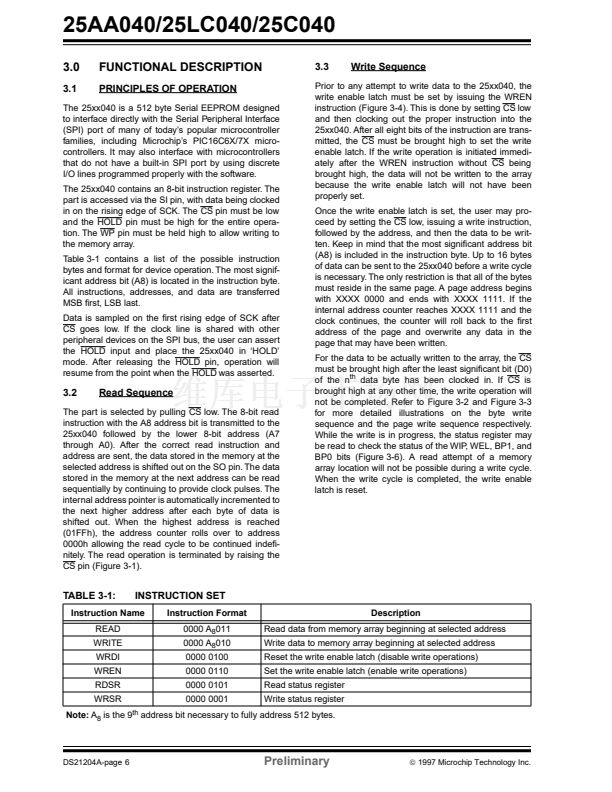
TABLE 3-1:
READ
WRITE
WRDI
WREN
RDSR
WRSR
INSTRUCTION SET
Instruction Format
0000 A
8
011
0000 A
8
010
0000 0100
0000 0110
0000 0101
0000 0001
Description
Read data from memory array beginning at selected address
Write data to memory array beginning at selected address
Reset the write enable latch (disable write operations)
Set the write enable latch (enable write operations)
Read status register
Write status register
Instruction Name
Note:
A
8
is the 9
th
address bit necessary to fully address 512 bytes.
DS21204A-page 6
Preliminary
漏
1997 Microchip Technology Inc.


 1
1
 2
2
 3
3
 4
4
 5
5
 6
6
 7
7
 8
8
 9
9
 10
10
 11
11
 12
12
