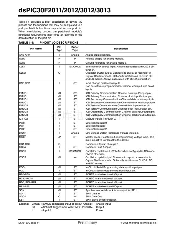
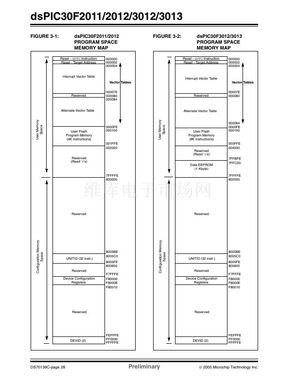
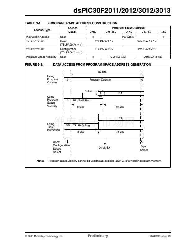
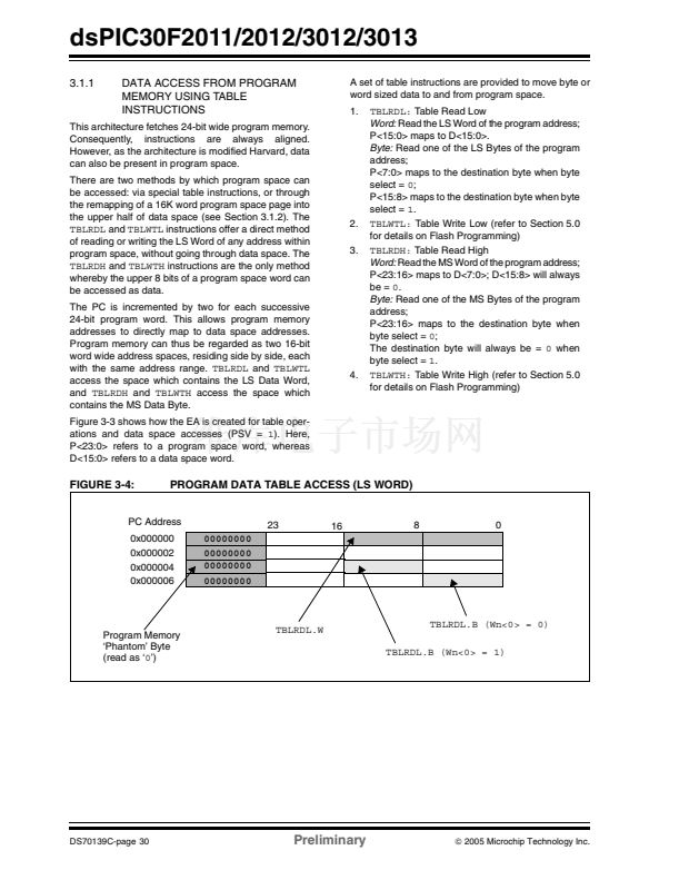
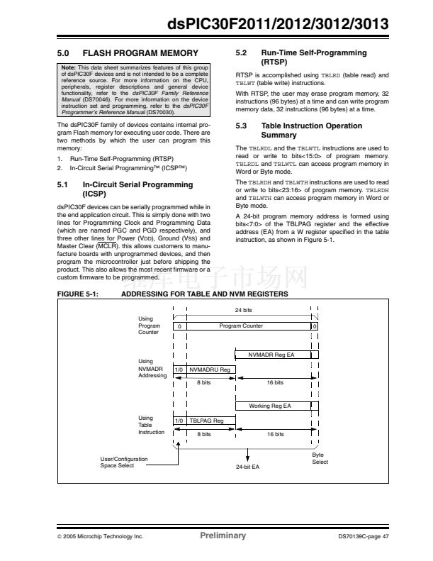
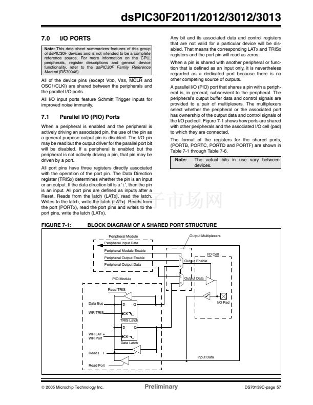
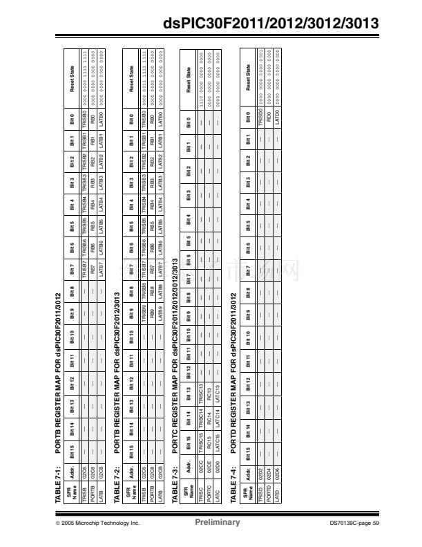
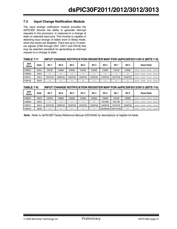
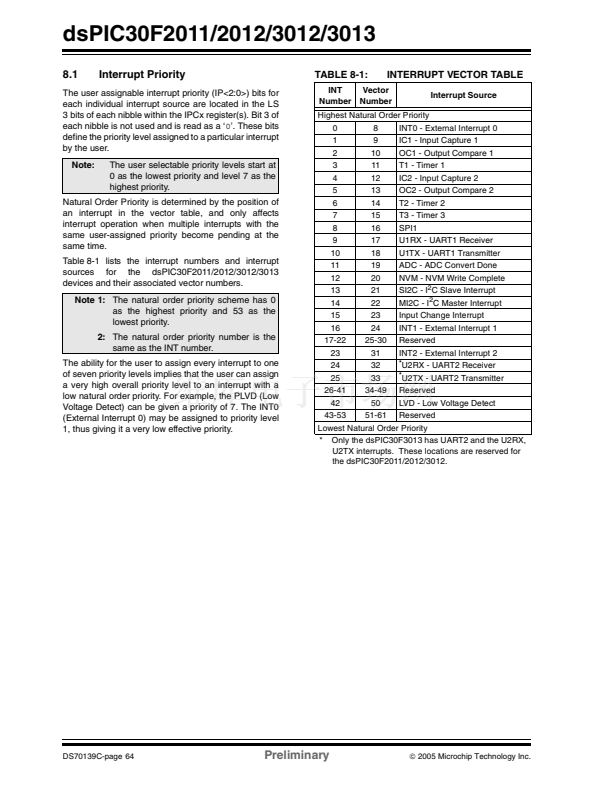
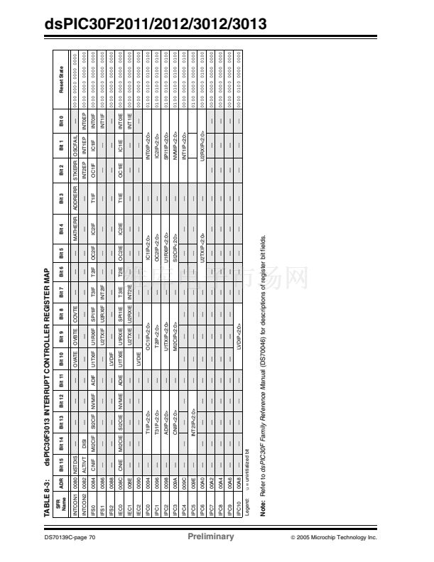
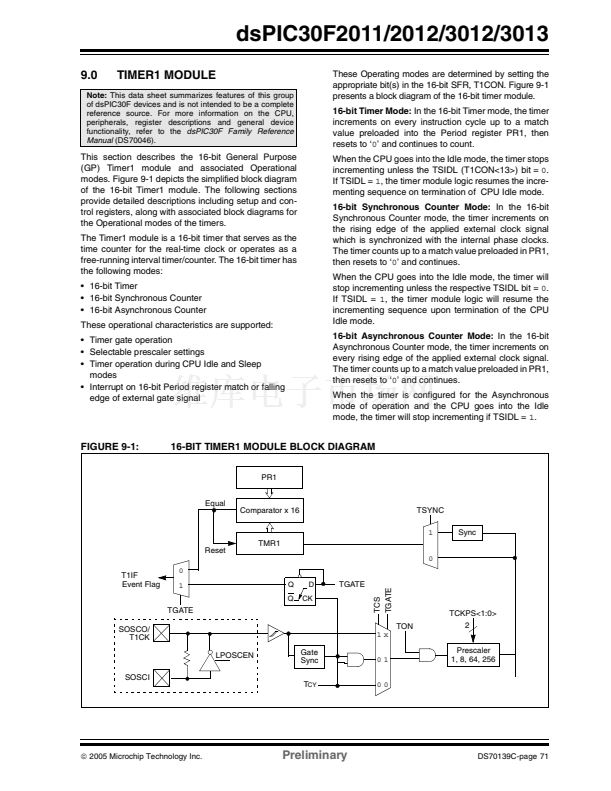
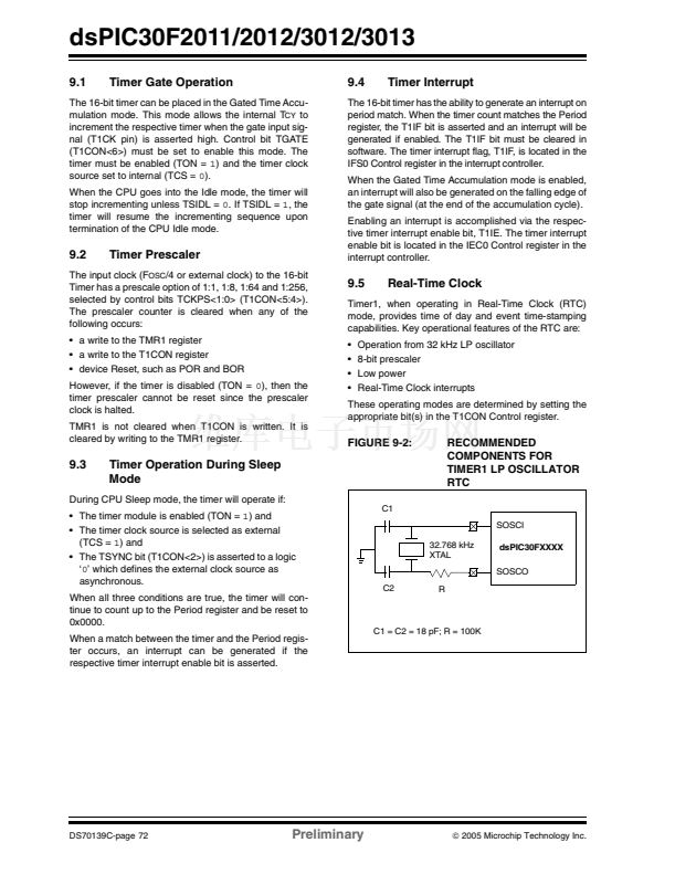
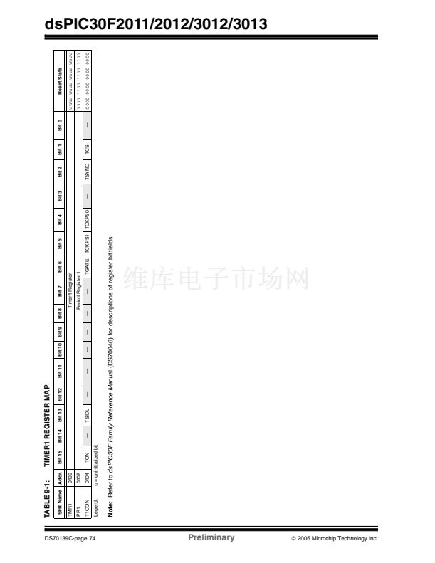
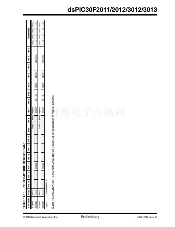
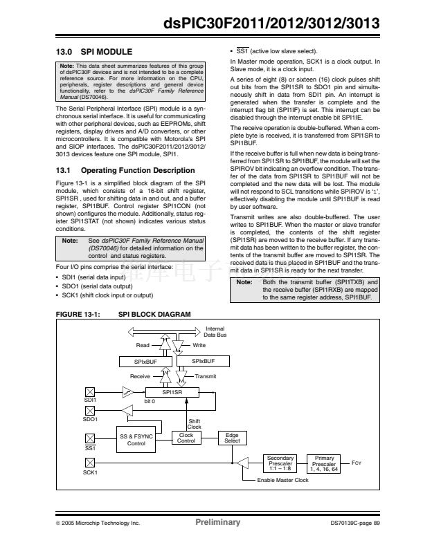
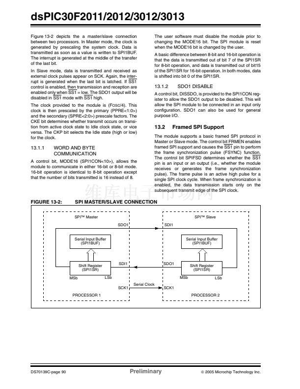
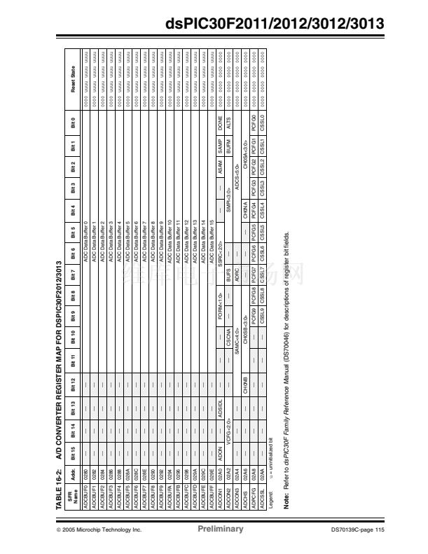
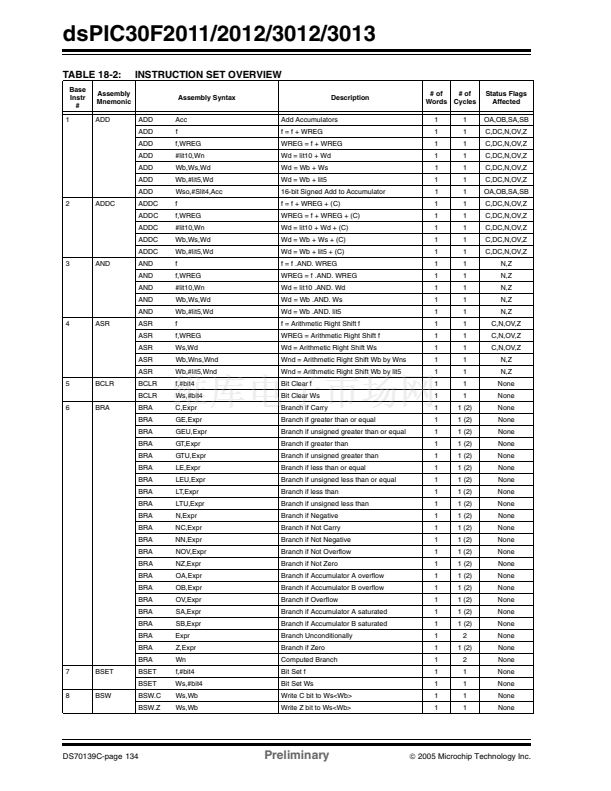
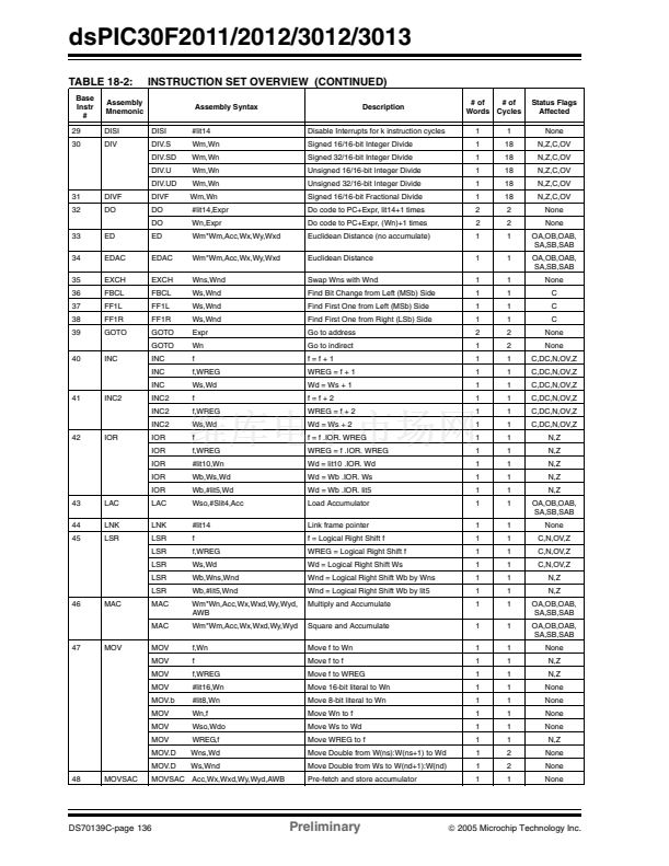
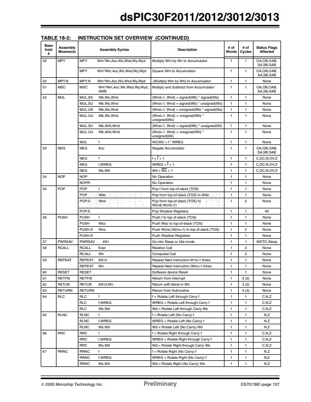
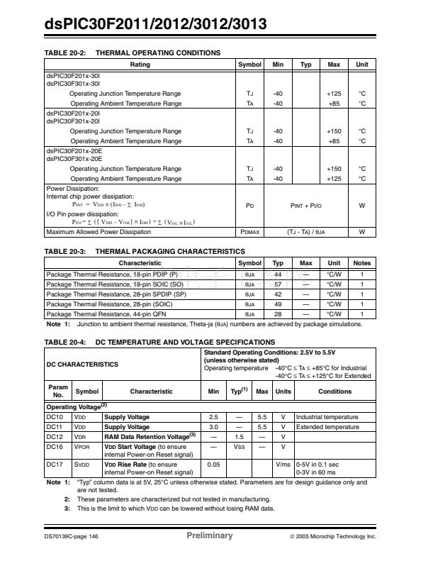
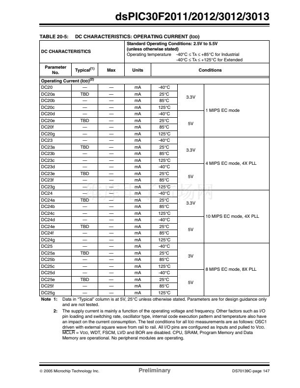
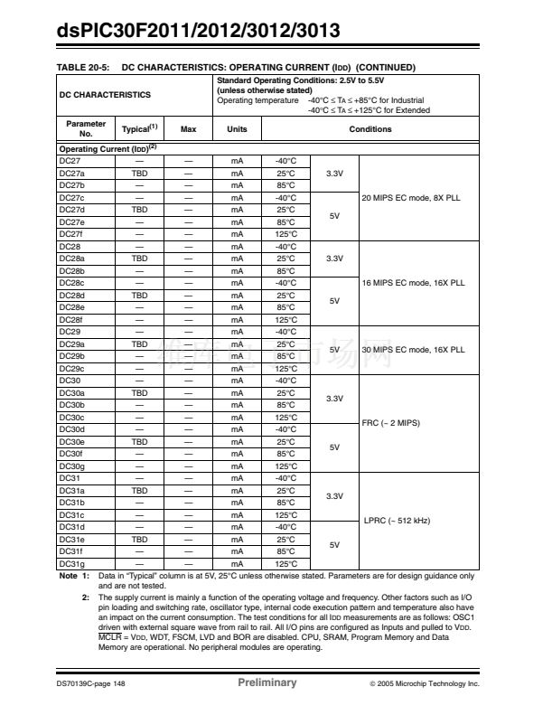
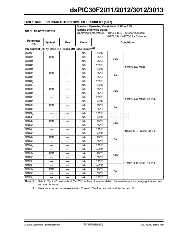
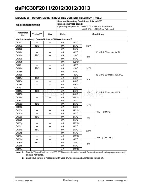
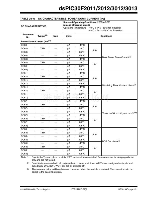
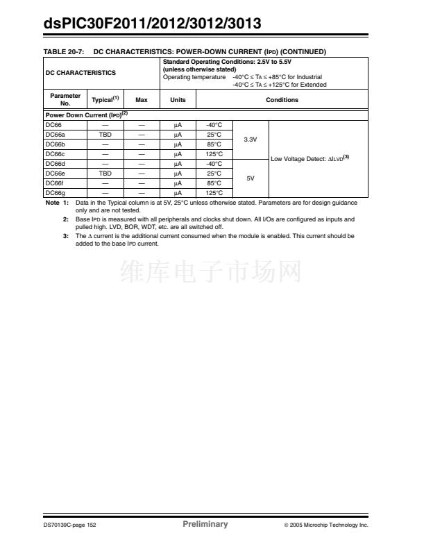
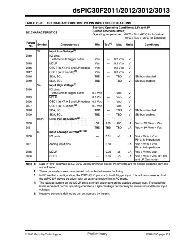
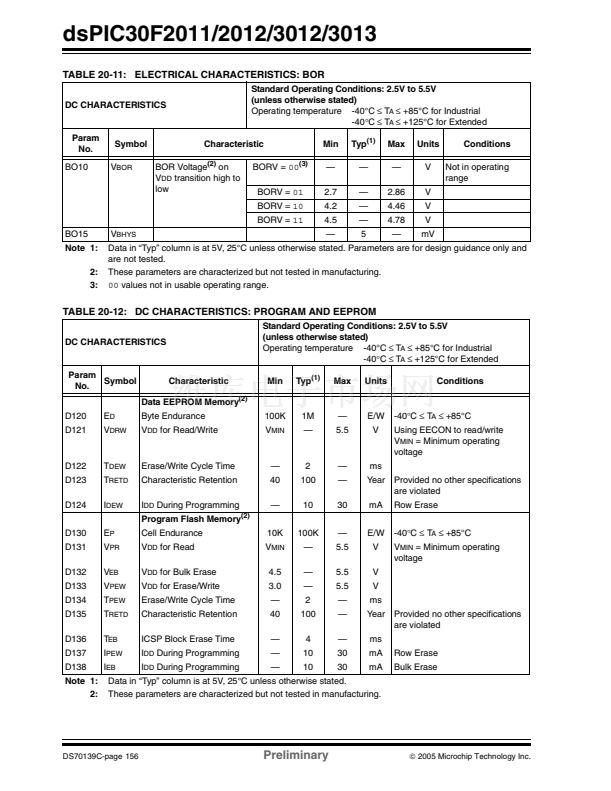
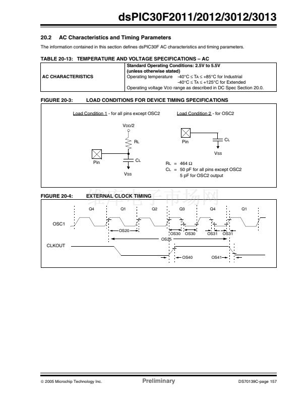
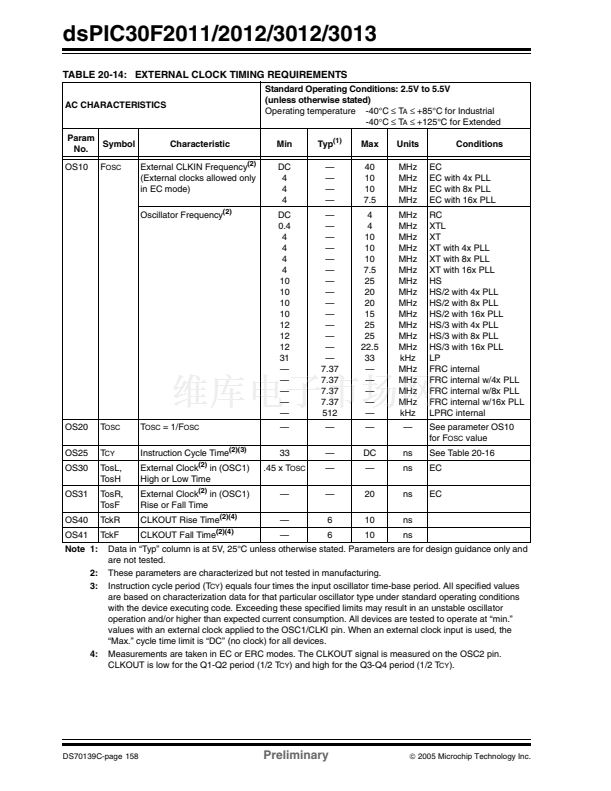
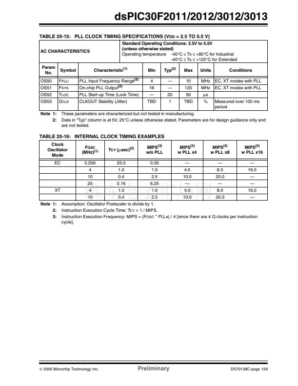
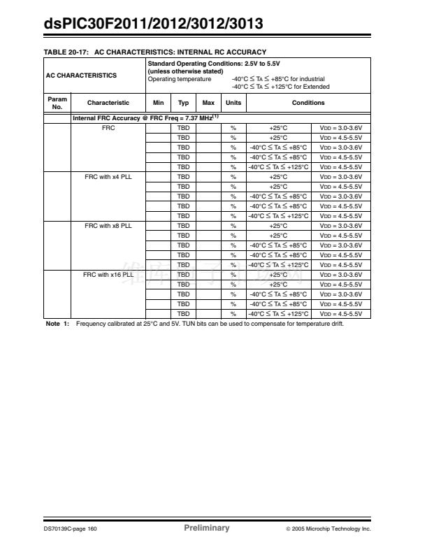
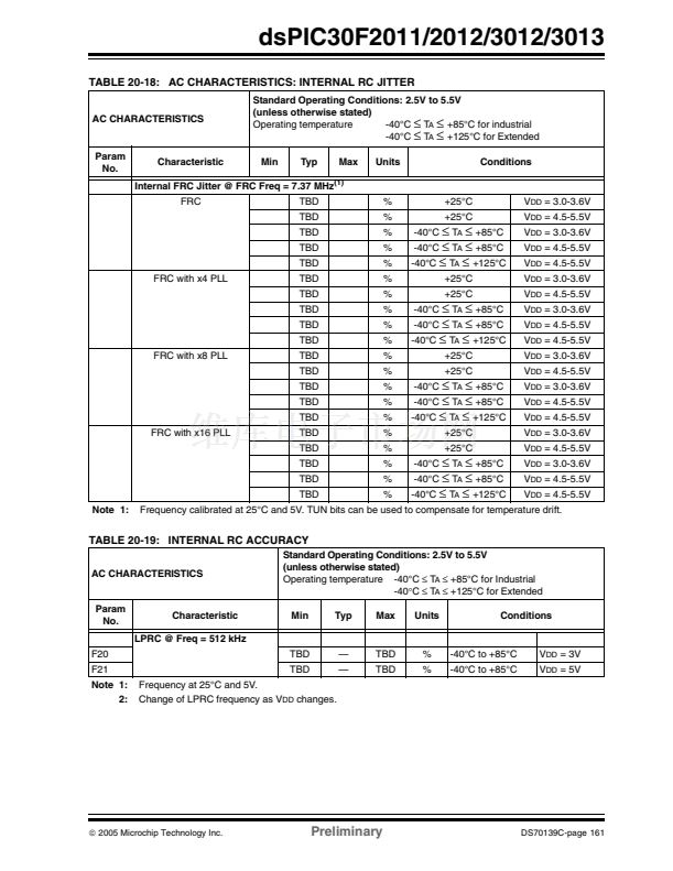
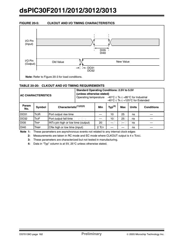
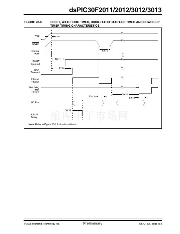
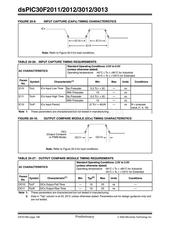
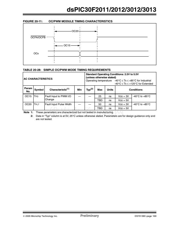
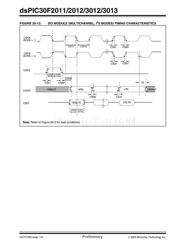
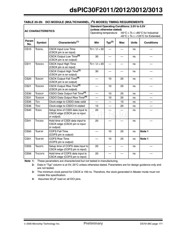
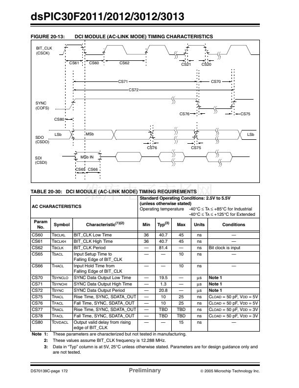
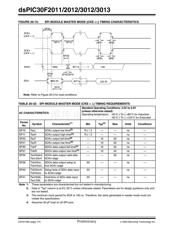
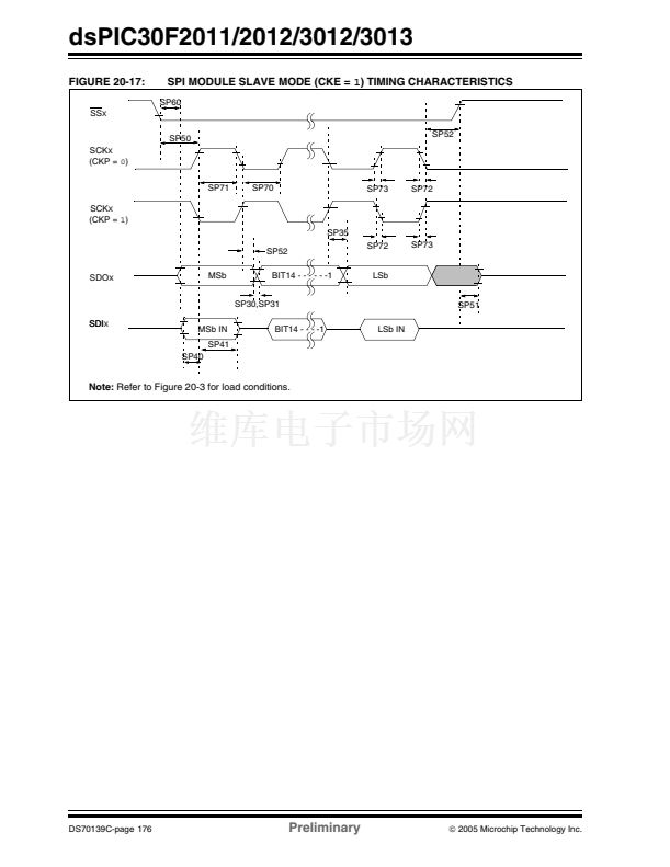
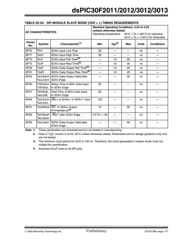
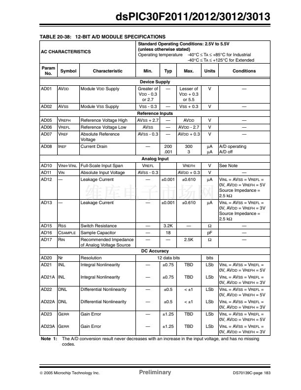
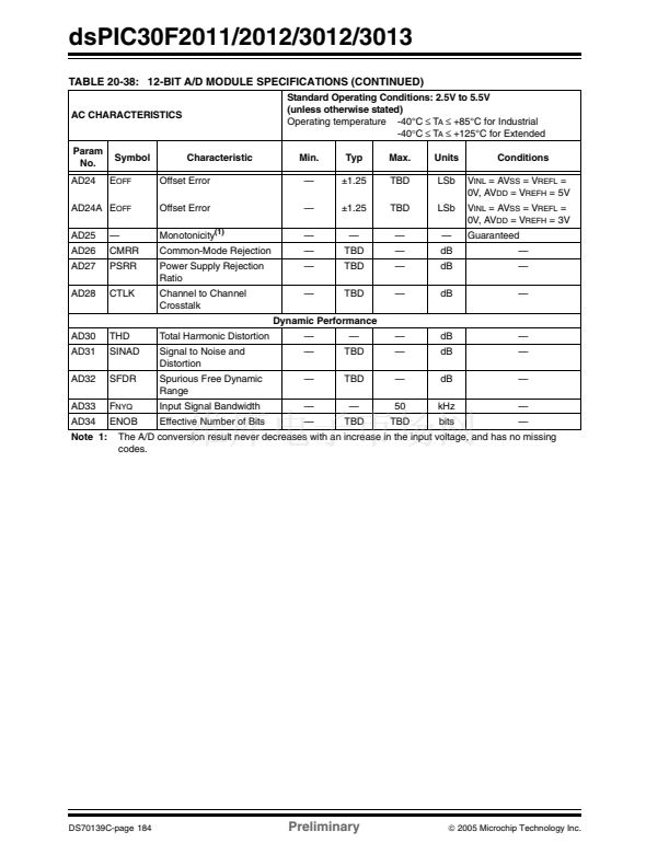
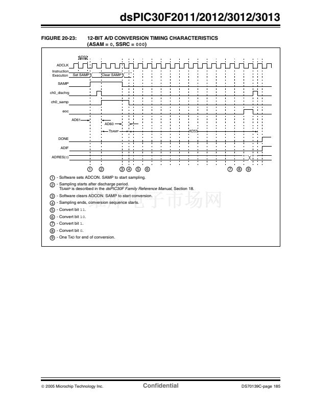
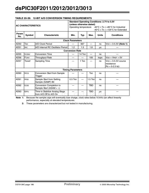
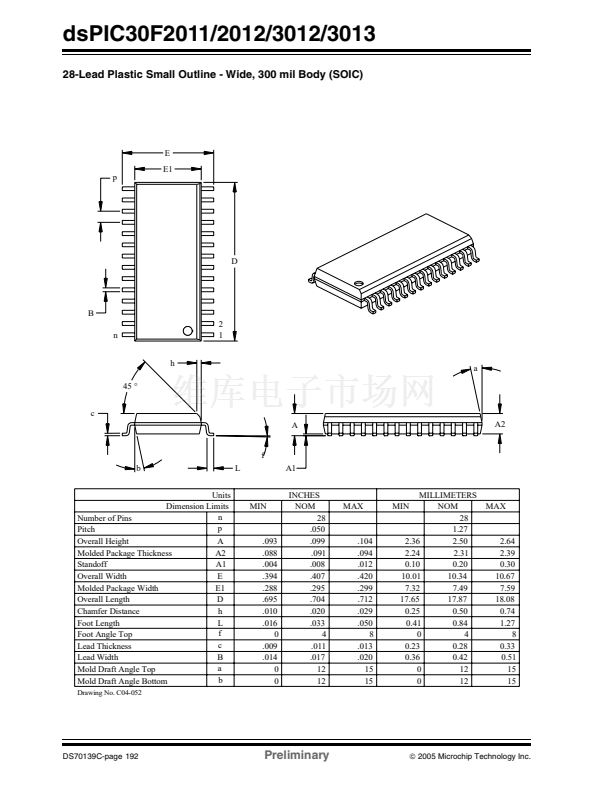
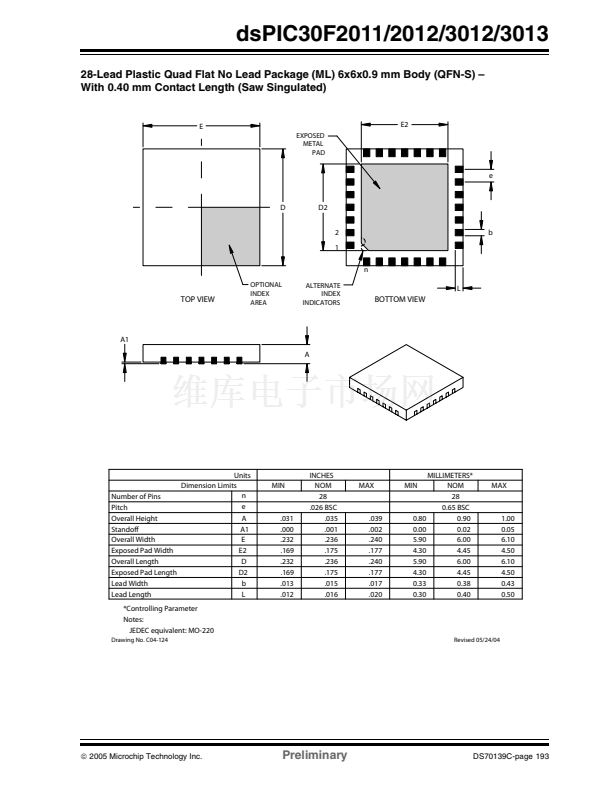
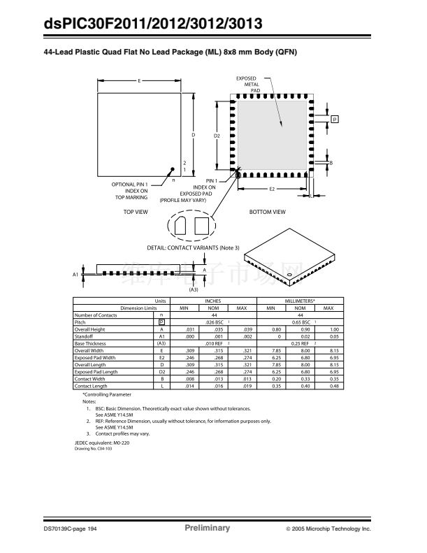
dsPIC30F2011/2012/3012/3013
7.2
Configuring Analog Port Pins
7.2.1
I/O PORT WRITE/READ TIMING
The use of the ADPCFG and TRIS registers control the
operation of the A/D port pins. The port pins that are
desired as analog inputs must have their correspond-
ing TRIS bit set (input). If the TRIS bit is cleared
(output), the digital output level (V
OH
or V
OL
) will be
converted.
When reading the Port register, all pins configured as
analog input channels will read as cleared (a low level).
Pins configured as digital inputs will not convert an ana-
log input. Analog levels on any pin that is defined as a
digital input (including the ANx pins) may cause the
input buffer to consume current that exceeds the
device specifications.
One instruction cycle is required between a port
direction change or port write operation and a read
operation of the same port. Typically this instruction
would be a
NOP.
EXAMPLE 7-1:
#0xF0, W0;
;
MOV W0, TRISB;
NOP
;
btss PORTB, #7;
MOV
PORT WRITE/READ
EXAMPLE
Configure PORTB<7:4>
as inputs
and PORTB<3:0> as outputs
additional instruction cycle
bit test RB7 and skip if set
DS70139C-page 58
Preliminary
漏
2005 Microchip Technology Inc.


 1
1
 2
2
 3
3
 4
4
 5
5
 6
6
 7
7
 8
8
 9
9
 10
10
 11
11
 12
12
 13
13
 14
14
 15
15
 16
16
 17
17
 18
18
 19
19
 20
20
 21
21
 22
22
 23
23
 24
24
 25
25
 26
26
 27
27
 28
28
 29
29
 30
30
 31
31
 32
32
 33
33
 34
34
 35
35
 36
36
 37
37
 38
38
 39
39
 40
40
 41
41
 42
42
 43
43
 44
44
 45
45
 46
46
 47
47
 48
48
 49
49
 50
50
 51
51
 52
52
 53
53
 54
54
 55
55
 56
56
 57
57
 58
58
 59
59
 60
60
 61
61
 62
62
 63
63
 64
64
 65
65
 66
66
 67
67
 68
68
 69
69
 70
70
 71
71
 72
72
 73
73
 74
74
 75
75
 76
76
 77
77
 78
78
 79
79
 80
80
 81
81
 82
82
 83
83
 84
84
 85
85
 86
86
 87
87
 88
88
 89
89
 90
90
 91
91
 92
92
 93
93
 94
94
 95
95
 96
96
 97
97
 98
98
 99
99
 100
100
 101
101
 102
102
 103
103
 104
104
 105
105
 106
106
 107
107
 108
108
 109
109
 110
110
 111
111
 112
112
 113
113
 114
114
 115
115
 116
116
 117
117
 118
118
 119
119
 120
120
 121
121
 122
122
 123
123
 124
124
 125
125
 126
126
 127
127
 128
128
 129
129
 130
130
 131
131
 132
132
 133
133
 134
134
 135
135
 136
136
 137
137
 138
138
 139
139
 140
140
 141
141
 142
142
 143
143
 144
144
 145
145
 146
146
 147
147
 148
148
 149
149
 150
150
 151
151
 152
152
 153
153
 154
154
 155
155
 156
156
 157
157
 158
158
 159
159
 160
160
 161
161
 162
162
 163
163
 164
164
 165
165
 166
166
 167
167
 168
168
 169
169
 170
170
 171
171
 172
172
 173
173
 174
174
 175
175
 176
176
 177
177
 178
178
 179
179
 180
180
 181
181
 182
182
 183
183
 184
184
 185
185
 186
186
 187
187
 188
188
 189
189
 190
190
 191
191
 192
192
 193
193
 194
194
 195
195
 196
196
 197
197
 198
198
 199
199
 200
200
 201
201
 202
202
 203
203
 204
204
 205
205
 206
206
 207
207
