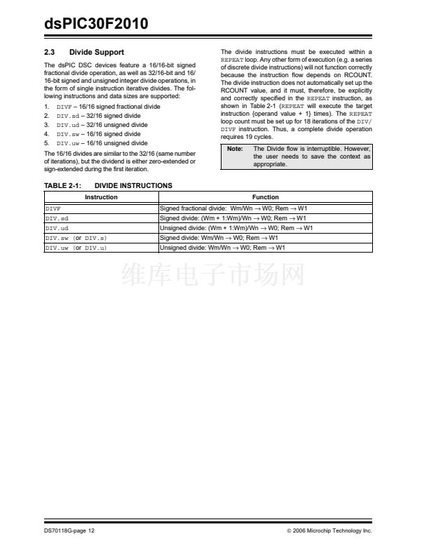
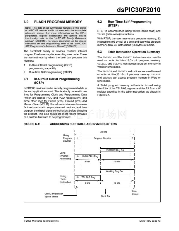
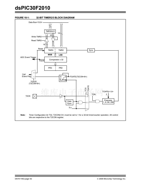
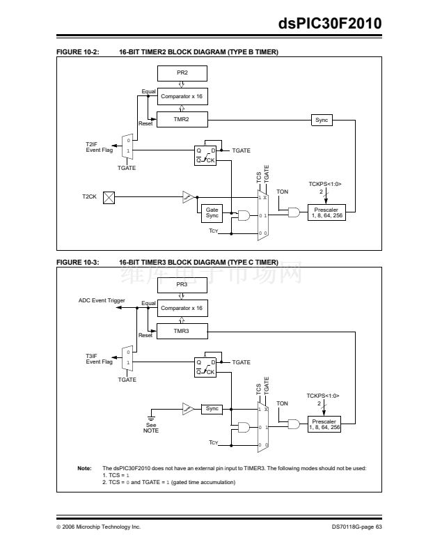
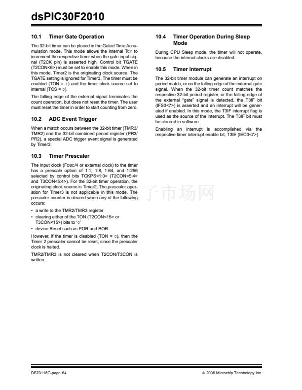
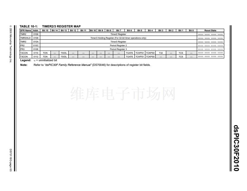
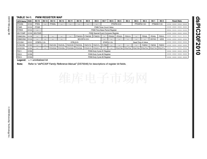
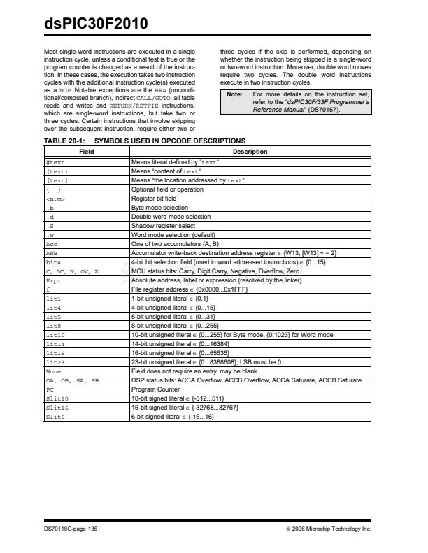
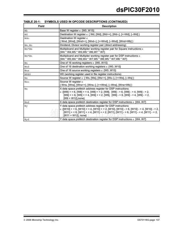
(DS70046). For more information on the device
33F Programmer鈥檚 Reference Manual鈥?/div>
(DS70157).
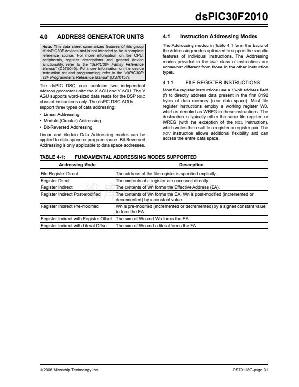
鈥?Linear indirect access of 32K word pages within
program space is also possible using any working
register, via table read and write instructions.
Table read and write instructions can be used to
access all 24 bits of an instruction word.
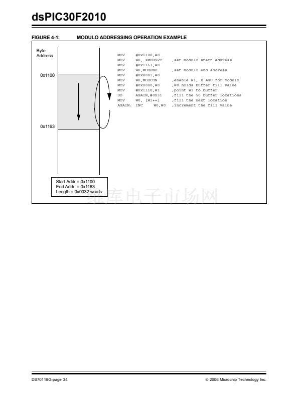
Overhead-free circular buffers (Modulo Addressing)
are supported in both X and Y address spaces. This is
primarily intended to remove the loop overhead for
DSP algorithms.
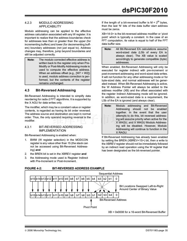
The X AGU also supports Bit-Reversed Addressing on
destination effective addresses, to greatly simplify input
or output data reordering for radix-2 FFT algorithms.
Refer to
Section 4.0 鈥淎ddress Generator Units鈥?/span>
for
details on Modulo and Bit-Reversed Addressing.
The core supports Inherent (no operand), Relative, Lit-
eral, Memory Direct, Register Direct, Register Indirect,
Register Offset and Literal Offset Addressing modes.
Instructions are associated with predefined Addressing
modes, depending upon their functional requirements.
For most instructions, the core is capable of executing
a data (or program data) memory read, a working reg-
ister (data) read, a data memory write and a program
(instruction) memory read per instruction cycle. As a
result, 3-operand instructions are supported, allowing
C = A + B operations to be executed in a single cycle.
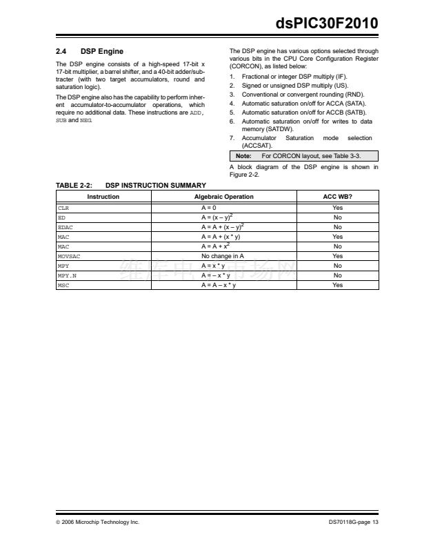
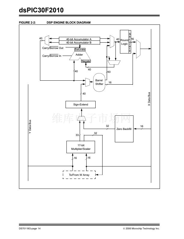
A DSP engine has been included to significantly
enhance the core arithmetic capability and throughput.
It features a high-speed 17-bit by 17-bit multiplier, a
40-bit ALU, two 40-bit saturating accumulators and a
40-bit bidirectional barrel shifter. Data in the accumula-
tor or any working register can be shifted up to 15 bits
right or 16 bits left in a single cycle. The DSP instruc-
tions operate seamlessly with all other instructions and
have been designed for optimal real-time performance.
The
MAC
class of instructions can concurrently fetch
two data operands from memory, while multiplying two
W registers. To enable this concurrent fetching of data
operands, the data space has been split for these
instructions and linear for all others. This has been
achieved in a transparent and flexible manner, by
dedicating certain working registers to each address
space for the
MAC
class of instructions.
The core does not support a multi-stage instruction
pipeline. However, a single stage instruction prefetch
mechanism is used, which accesses and partially
decodes instructions a cycle ahead of execution, in
order to maximize available execution time. Most
instructions execute in a single cycle, with certain
exceptions.
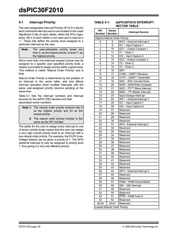
The core features a vectored exception processing
structure for traps and interrupts, with 62 independent
vectors. The exceptions consist of up to 8 traps (of
which 4 are reserved) and 54 interrupts. Each interrupt
is prioritized based on a user-assigned priority between
1 and 7 (1 being the lowest priority and 7 being the
highest) in conjunction with a predetermined 鈥榥atural
order鈥? Traps have fixed priorities, ranging from 8 to 15.
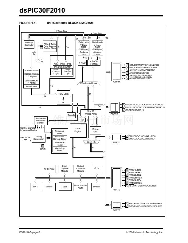
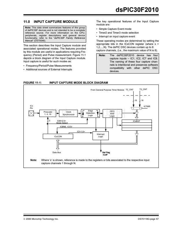
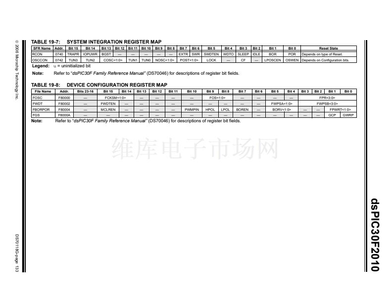
This document provides a summary of the
dsPIC30F2010 CPU and peripheral function. For a
complete description of this functionality, please refer
to the 鈥渄sPIC30F
Family Reference Manual鈥?/div>
(DS70046).
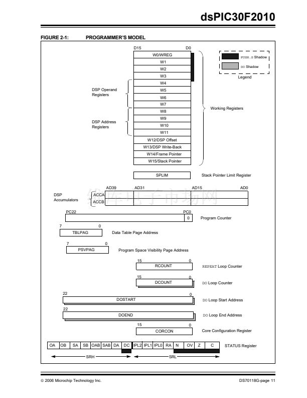
2.1
Core Overview
The core has a 24-bit instruction word. The Program
Counter (PC) is 23 bits wide with the Least Significant
bit (LSb) always clear (see
Section 3.1 鈥淧rogram
Address Space鈥?,
and the Most Significant bit (MSb)
is ignored during normal program execution, except for
certain specialized instructions. Thus, the PC can
address up to 4M instruction words of user program
space. An instruction prefetch mechanism is used to
help maintain throughput. Program loop constructs,
free from loop count management overhead, are sup-
ported using the
DO
and
REPEAT
instructions, both of
which are interruptible at any point.
The working register array consists of 16x16-bit regis-
ters, each of which can act as data, address or offset
registers. One working register (W15) operates as a
software Stack Pointer for interrupts and calls.
The data space is 64 Kbytes (32K words) and is split
into two blocks, referred to as X and Y data memory.
Each block has its own independent Address Genera-
tion Unit (AGU). Most instructions operate solely
through the X memory AGU, which provides the
appearance of a single unified data space. The
Multiply-Accumulate (MAC) class of dual source DSP
instructions operate through both the X and Y AGUs,
splitting the data address space into two parts (see
Section 3.2 鈥淒ata Address Space鈥?.
The X and Y
data space boundary is device specific and cannot be
altered by the user. Each data word consists of 2 bytes,
and most instructions can address data either as words
or bytes.
There are two methods of accessing data stored in
program memory:
鈥?The upper 32 Kbytes of data space memory can be
mapped into the lower half (user space) of program
space at any 16K program word boundary, defined
by the 8-bit Program Space Visibility Page
(PSVPAG) register. This lets any instruction access
program space as if it were data space, with a limi-
tation that the access requires an additional cycle.
Moreover, only the lower 16 bits of each instruction
word can be accessed using this method.
漏
2006 Microchip Technology Inc.
DS70118G-page 9


 1
1
 2
2
 3
3
 4
4
 5
5
 6
6
 7
7
 8
8
 9
9
 10
10
 11
11
 12
12
 13
13
 14
14
 15
15
 16
16
 17
17
 18
18
 19
19
 20
20
 21
21
 22
22
 23
23
 24
24
 25
25
 26
26
 27
27
 28
28
 29
29
 30
30
 31
31
 32
32
 33
33
 34
34
 35
35
 36
36
 37
37
 38
38
 39
39
 40
40
 41
41
 42
42
 43
43
 44
44
 45
45
 46
46
 47
47
 48
48
 49
49
 50
50
 51
51
 52
52
 53
53
 54
54
 55
55
 56
56
 57
57
 58
58
 59
59
 60
60
 61
61
 62
62
 63
63
 64
64
 65
65
 66
66
 67
67
 68
68
 69
69
 70
70
 71
71
 72
72
 73
73
 74
74
 75
75
 76
76
 77
77
 78
78
 79
79
 80
80
 81
81
 82
82
 83
83
 84
84
 85
85
 86
86
 87
87
 88
88
 89
89
 90
90
 91
91
 92
92
 93
93
 94
94
 95
95
 96
96
 97
97
 98
98
 99
99
 100
100
 101
101
 102
102
 103
103
 104
104
 105
105
 106
106
 107
107
 108
108
 109
109
 110
110
 111
111
 112
112
 113
113
 114
114
 115
115
 116
116
 117
117
 118
118
 119
119
 120
120
 121
121
 122
122
 123
123
 124
124
 125
125
 126
126
 127
127
 128
128
 129
129
 130
130
 131
131
 132
132
 133
133
 134
134
 135
135
 136
136
 137
137
 138
138
 139
139
 140
140
 141
141
 142
142
 143
143
 144
144
 145
145
 146
146
 147
147
 148
148
 149
149
 150
150
 151
151
 152
152
 153
153
 154
154
 155
155
 156
156
 157
157
 158
158
 159
159
 160
160
 161
161
 162
162
 163
163
 164
164
 165
165
 166
166
 167
167
 168
168
 169
169
 170
170
 171
171
 172
172
 173
173
 174
174
 175
175
 176
176
 177
177
 178
178
 179
179
 180
180
 181
181
 182
182
 183
183
 184
184
 185
185
 186
186
 187
187
 188
188
 189
189
 190
190
 191
191
 192
192
 193
193
 194
194
 195
195
 196
196
 197
197
 198
198
 199
199
 200
200
 201
201
 202
202
 203
203
