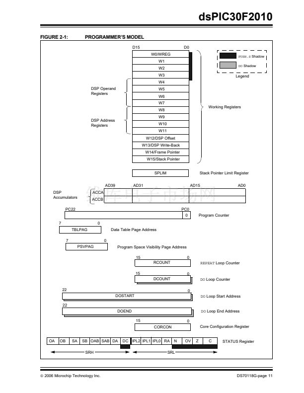
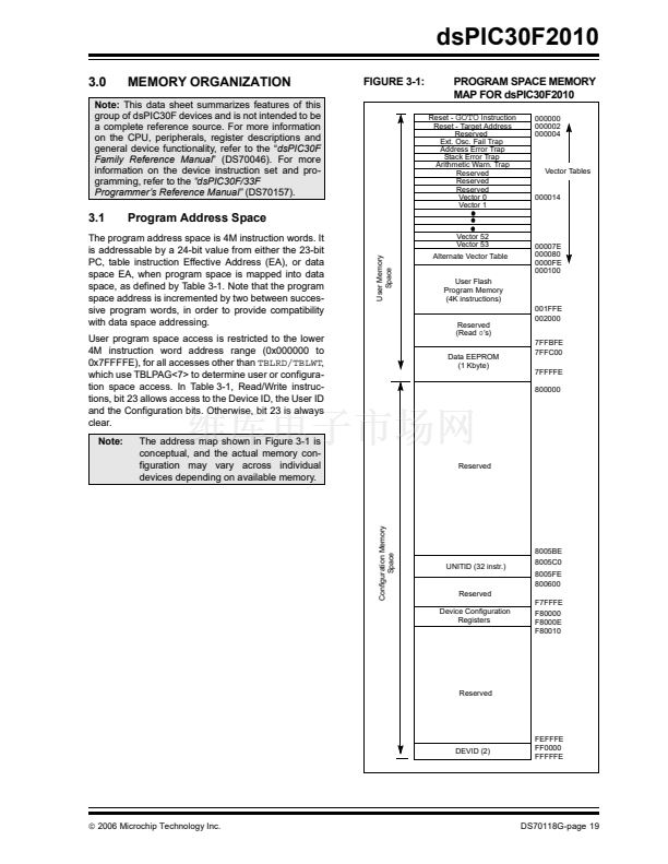
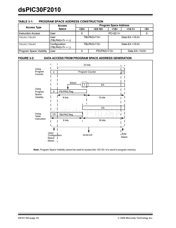
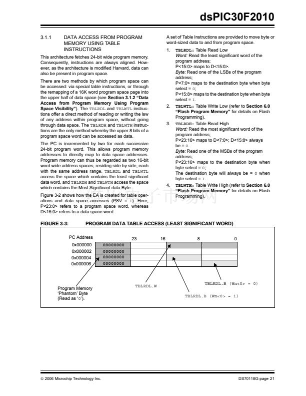
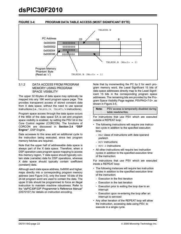
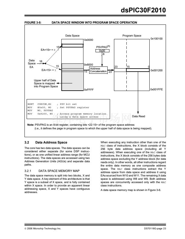
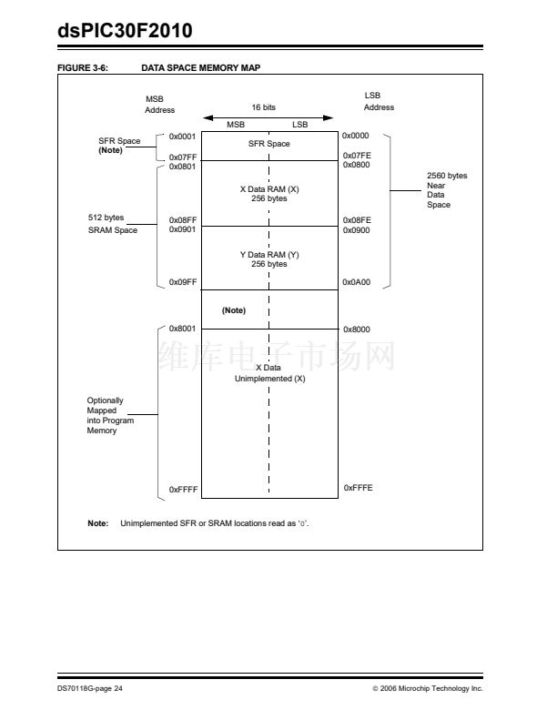
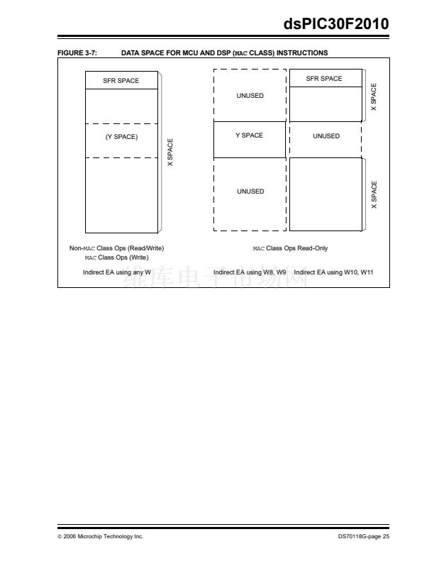
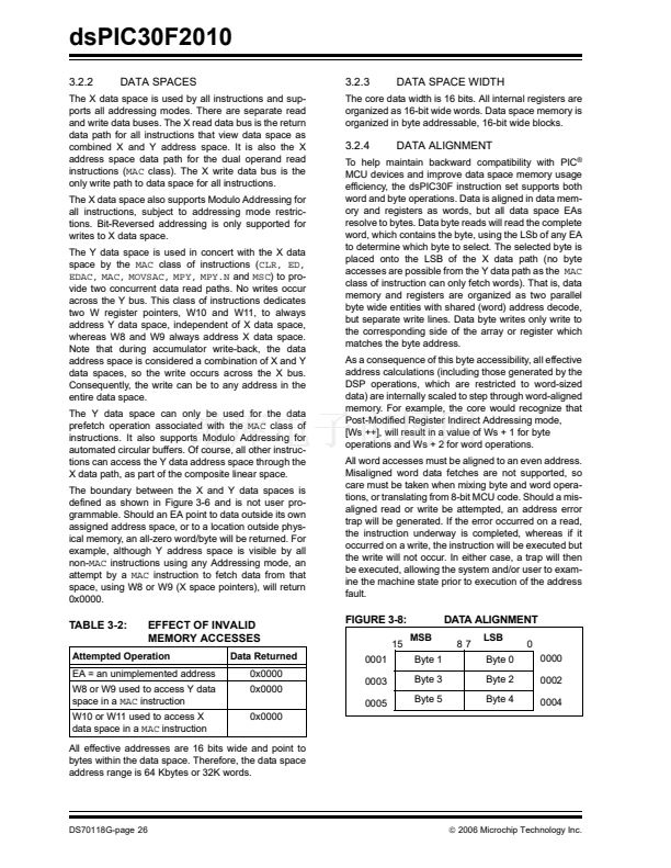
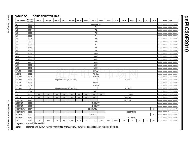
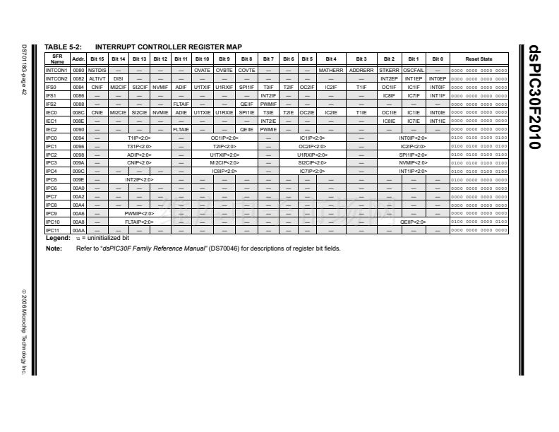
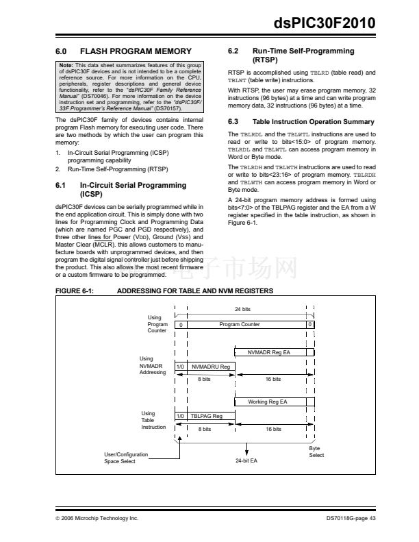
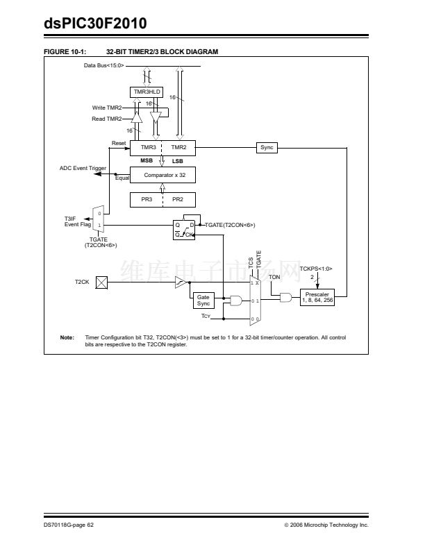
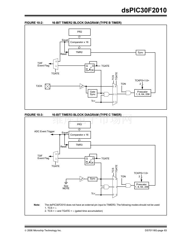
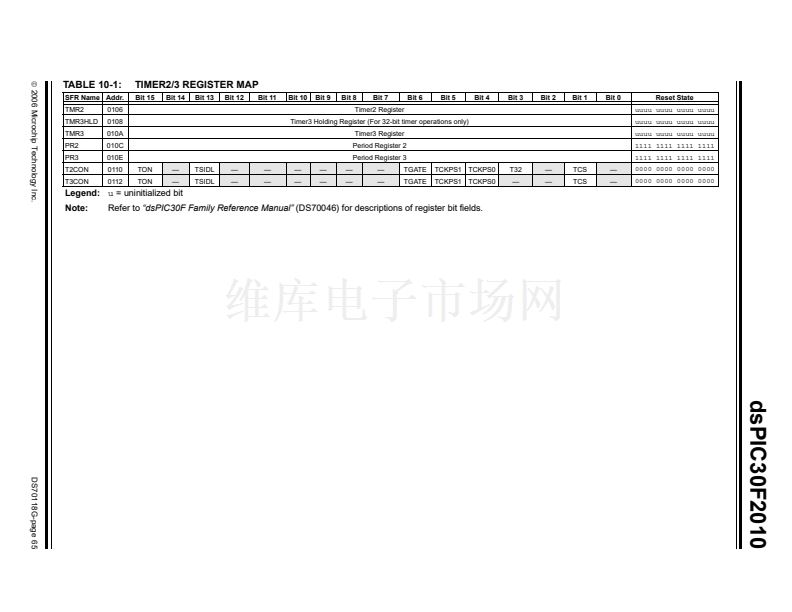
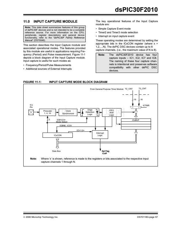
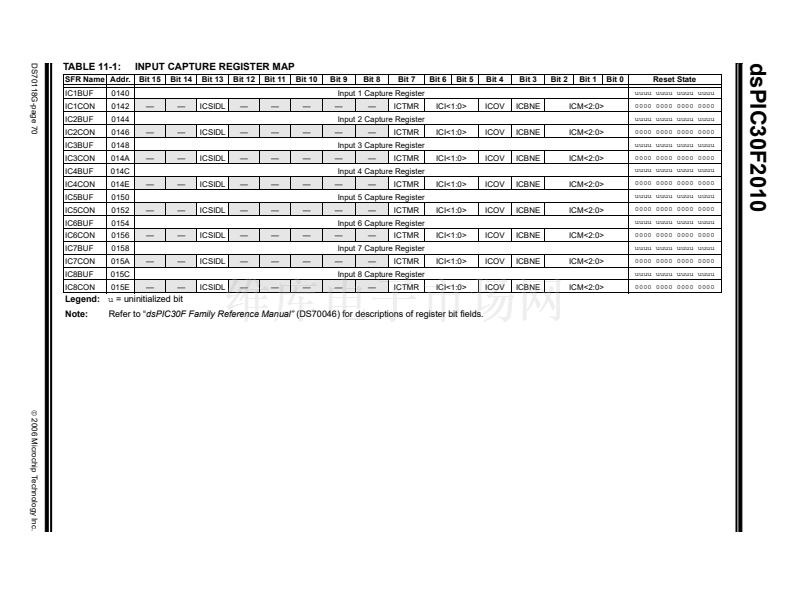
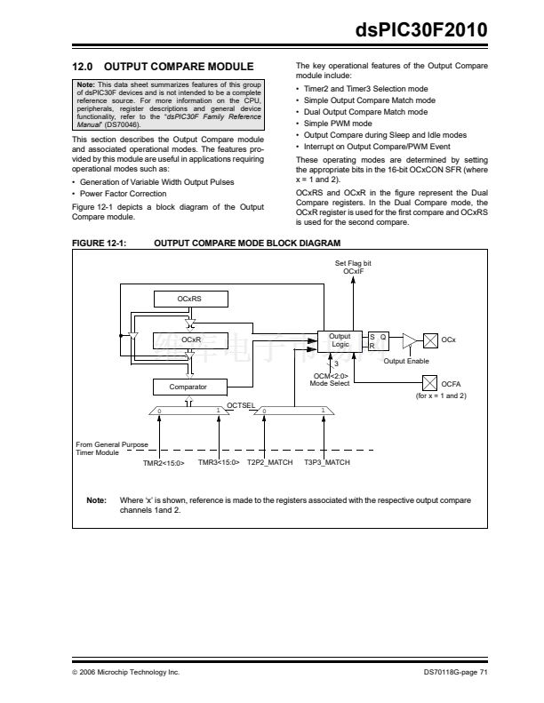
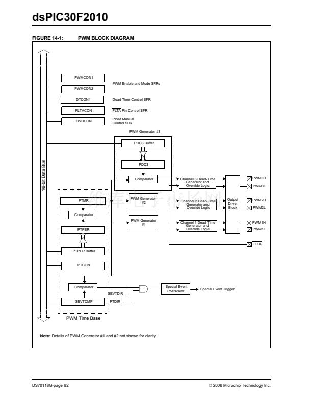
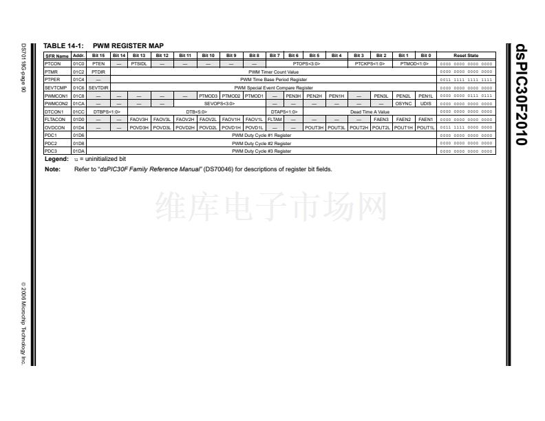
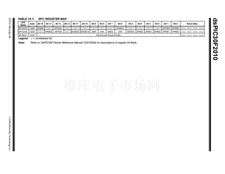
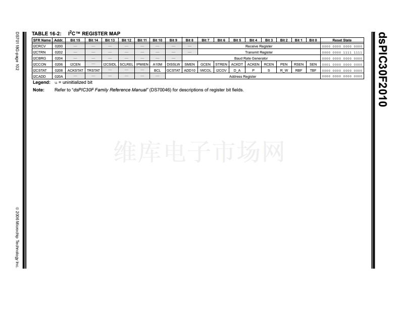
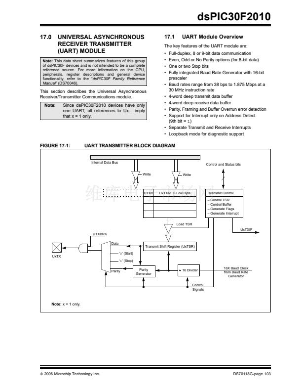
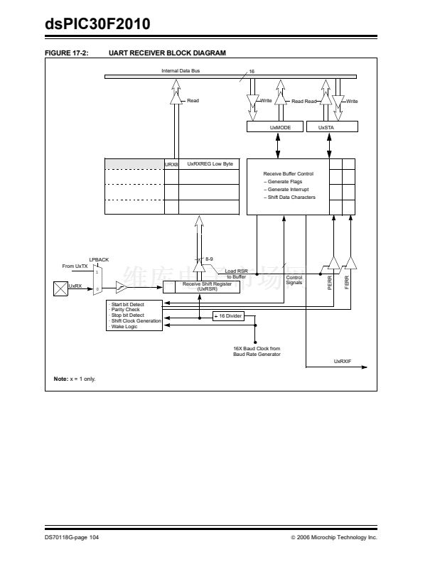
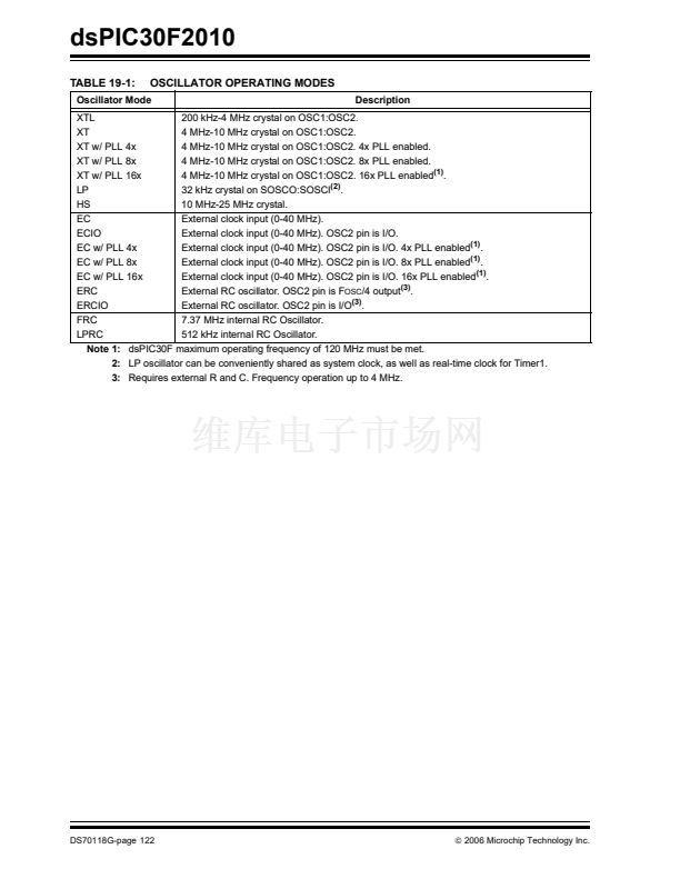
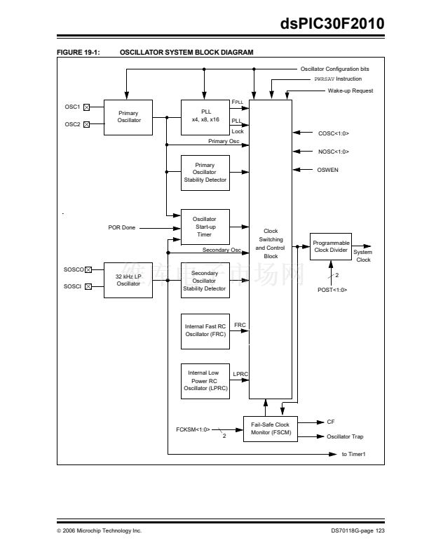
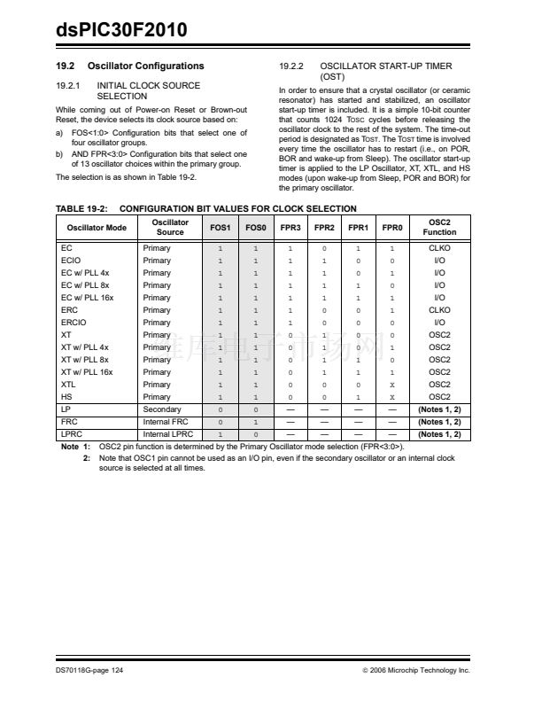
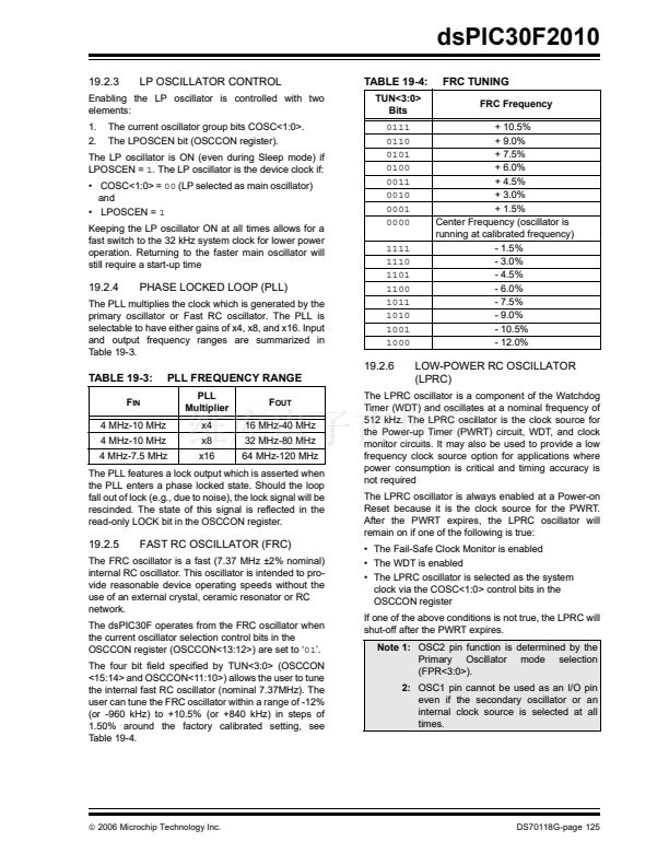
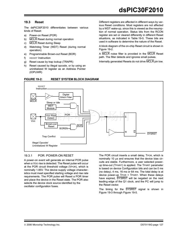
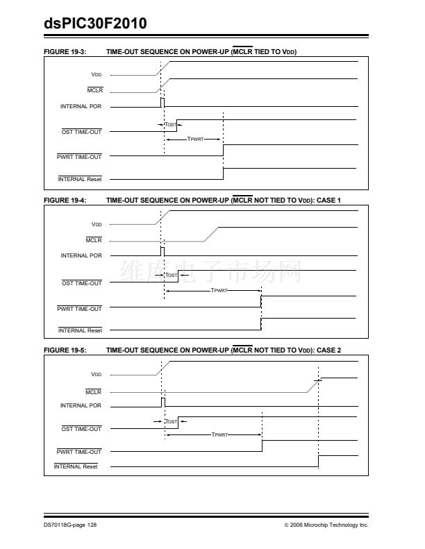
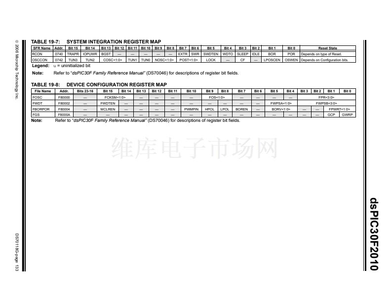
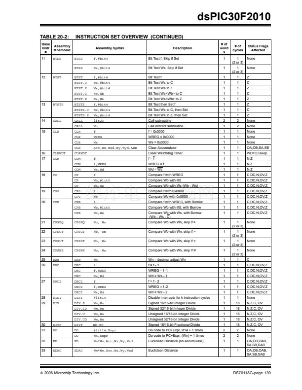
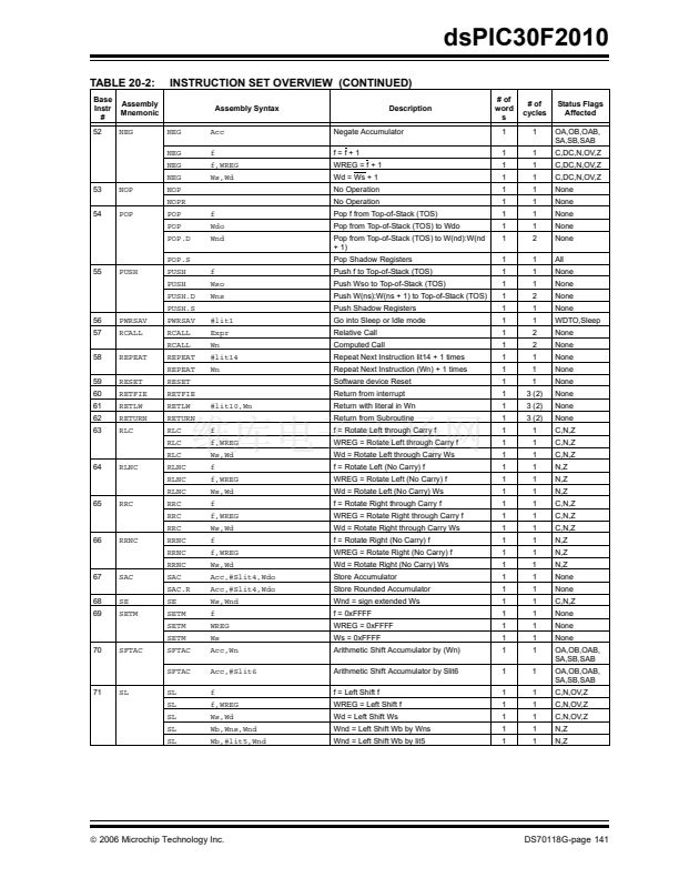
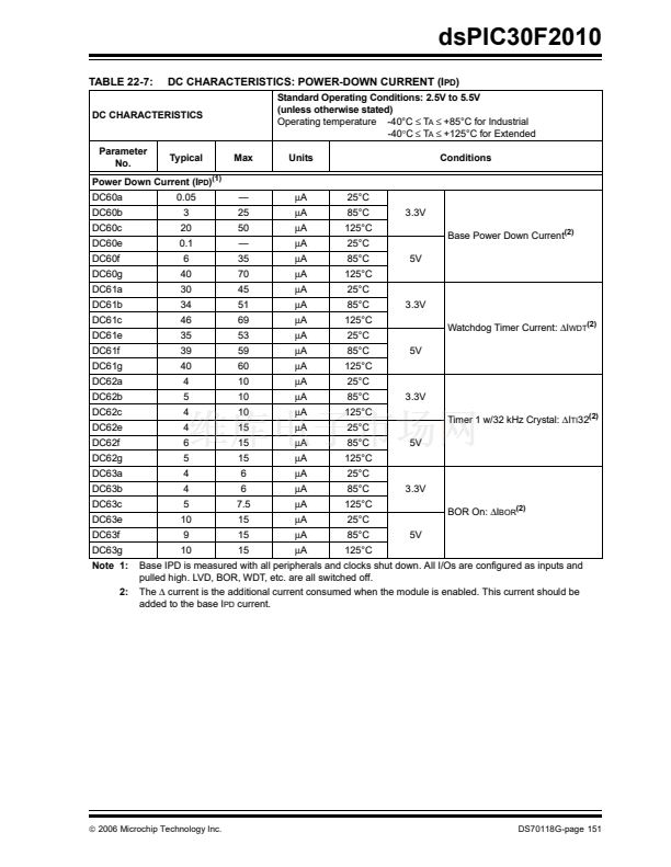
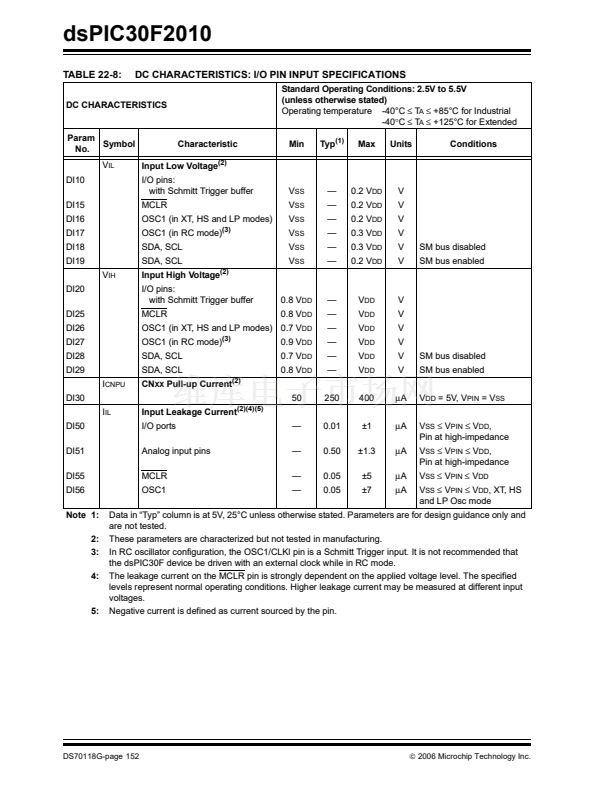
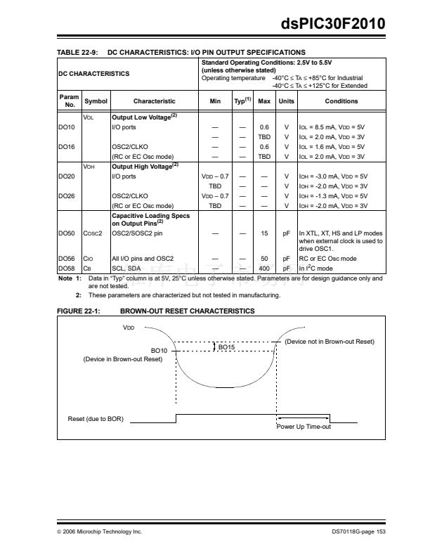
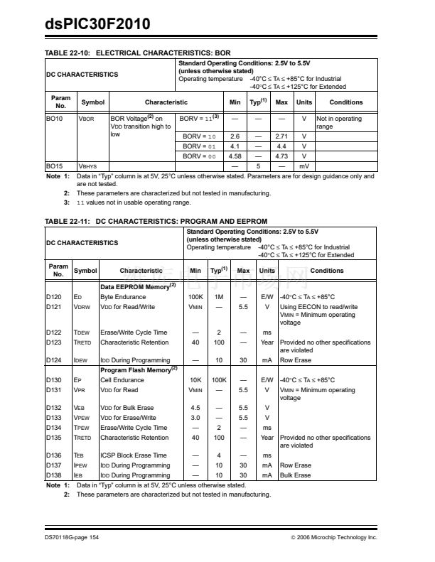
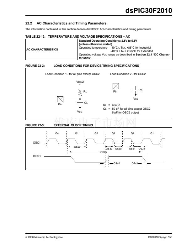
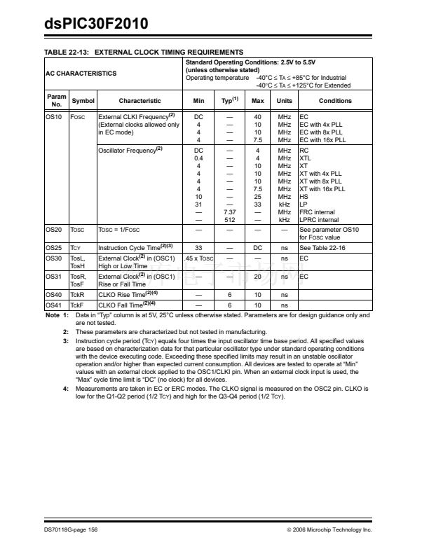
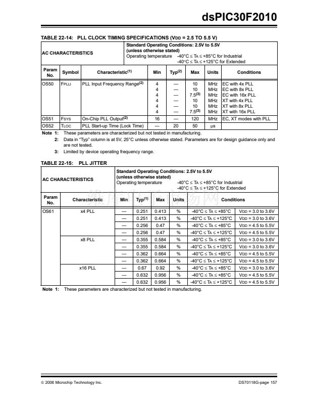
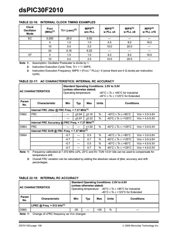
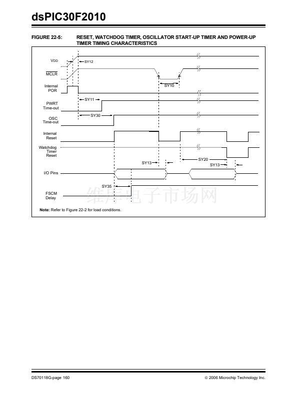
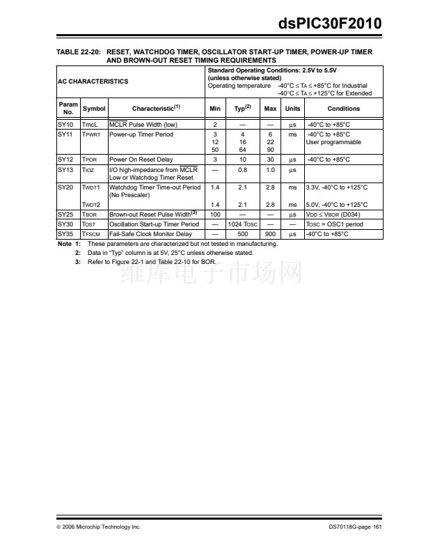
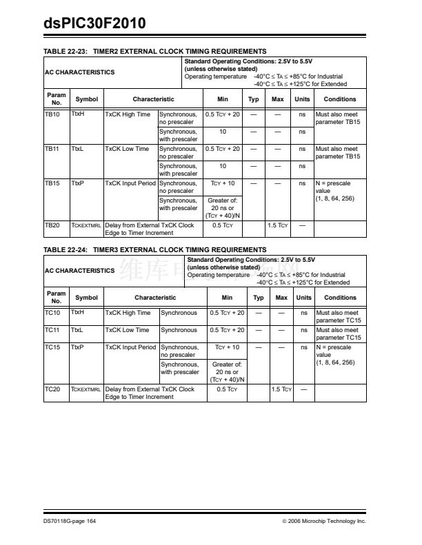
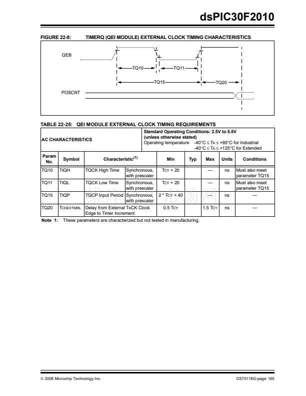
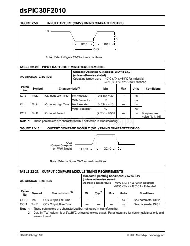
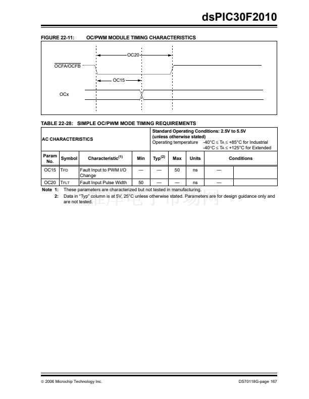
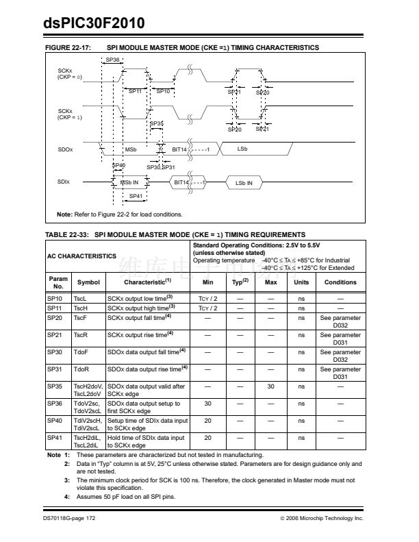
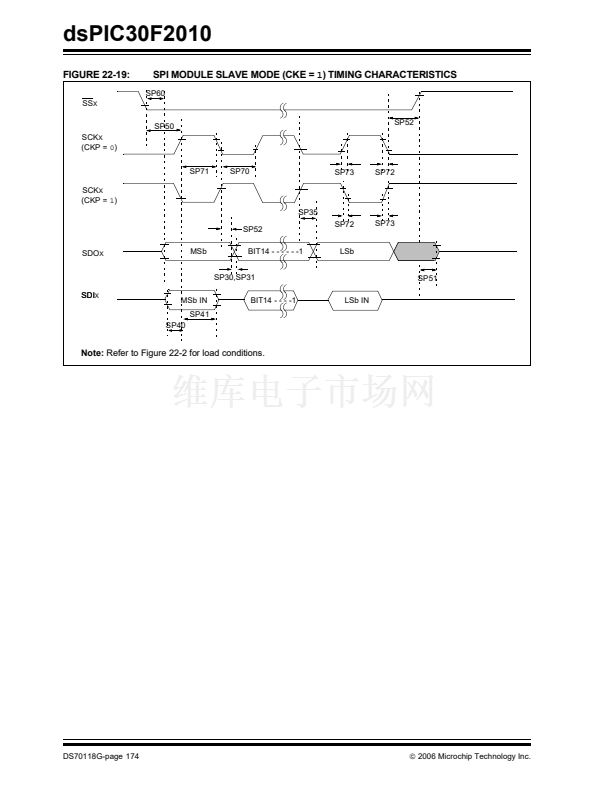
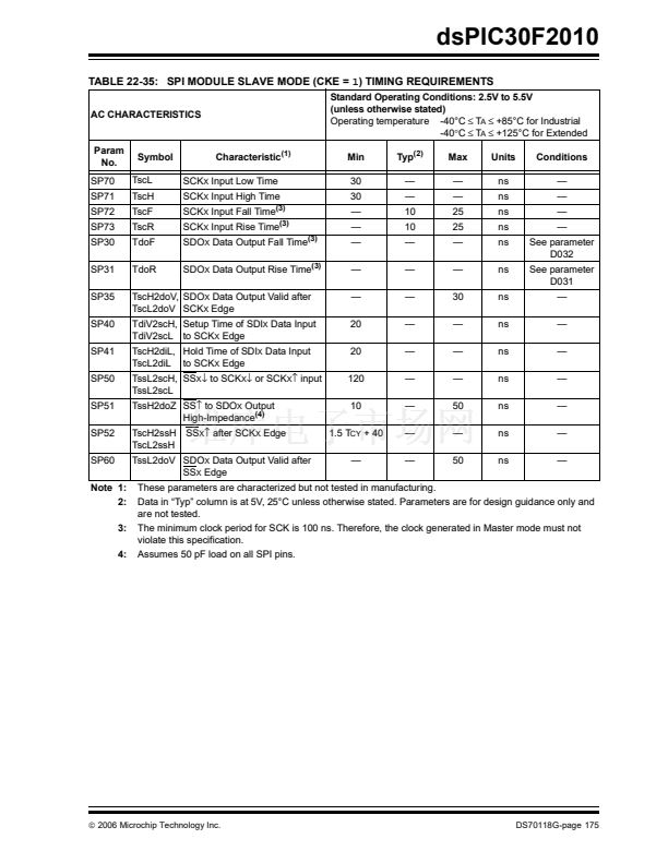
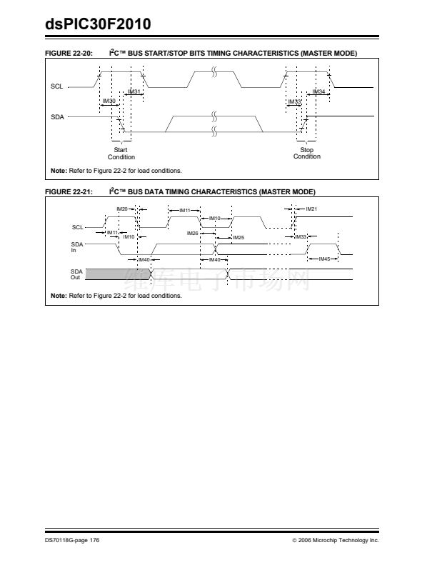
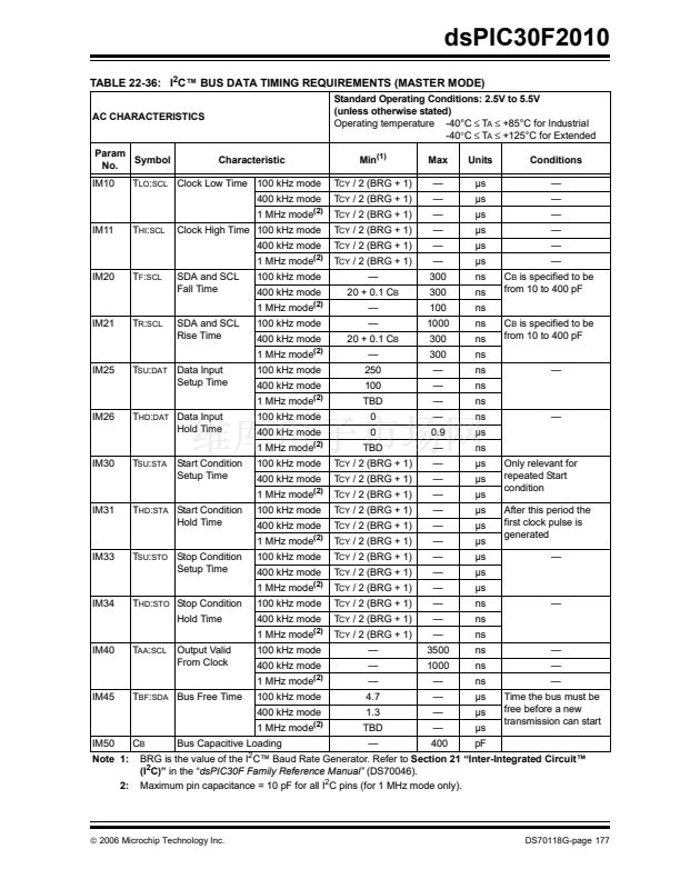
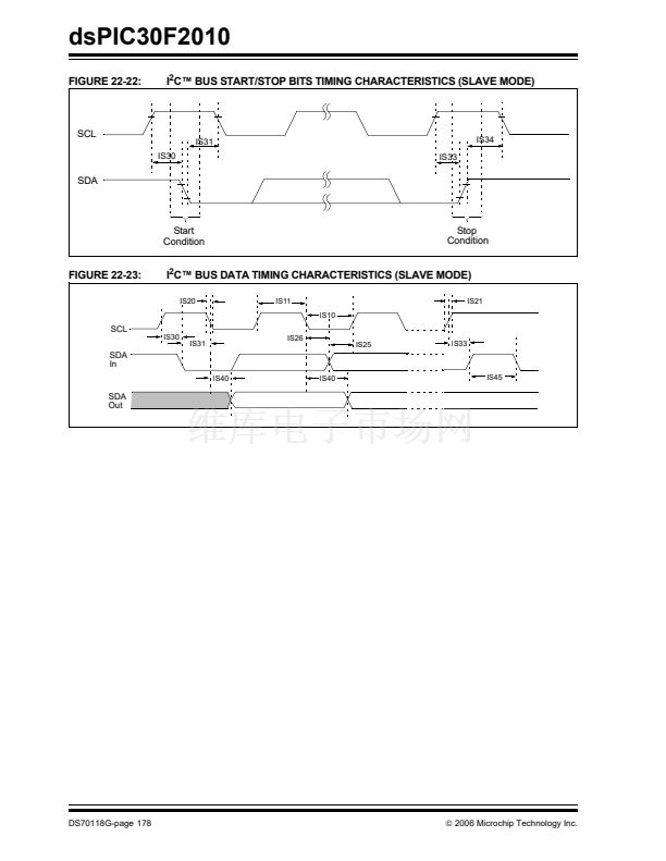
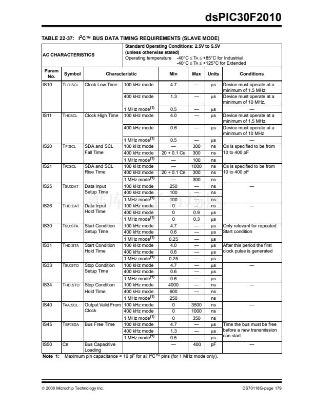
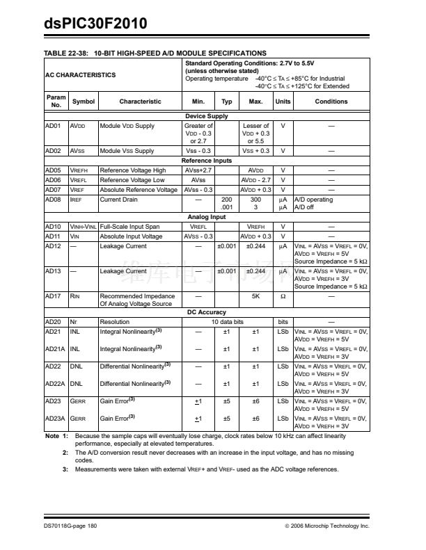
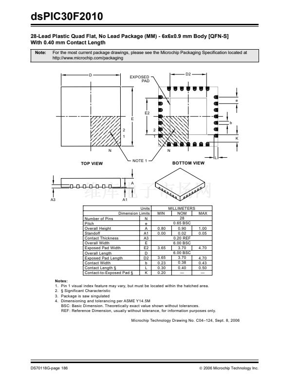
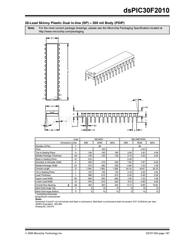
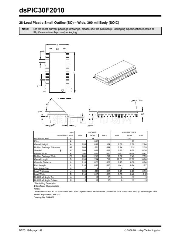
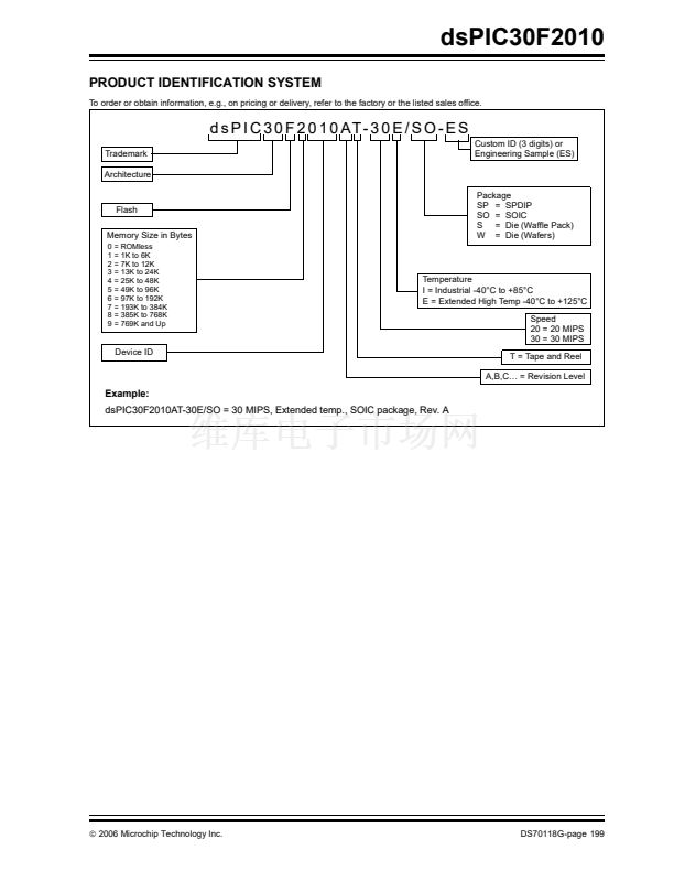
dsPIC30F2010
7.3.2
WRITING A BLOCK OF DATA
EEPROM
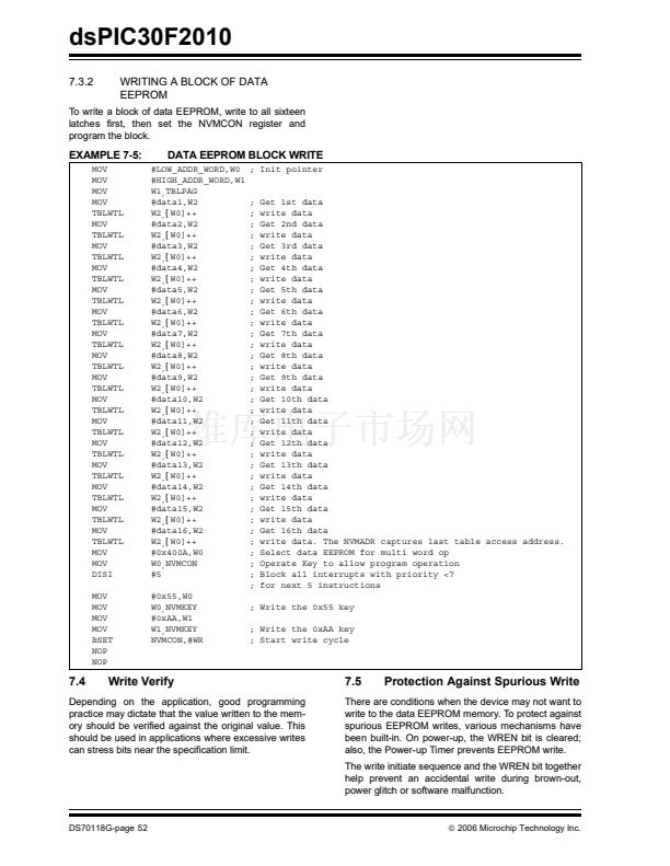
To write a block of data EEPROM, write to all sixteen
latches first, then set the NVMCON register and
program the block.
EXAMPLE 7-5:
MOV
MOV
MOV
MOV
TBLWTL
MOV
TBLWTL
MOV
TBLWTL
MOV
TBLWTL
MOV
TBLWTL
MOV
TBLWTL
MOV
TBLWTL
MOV
TBLWTL
MOV
TBLWTL
MOV
TBLWTL
MOV
TBLWTL
MOV
TBLWTL
MOV
TBLWTL
MOV
TBLWTL
MOV
TBLWTL
MOV
TBLWTL
MOV
MOV
DISI
MOV
MOV
MOV
MOV
BSET
NOP
NOP
DATA EEPROM BLOCK WRITE
#LOW_ADDR_WORD,W0
#HIGH_ADDR_WORD,W1
W1
,
TBLPAG
#data1,W2
W2
,
[
W0]++
#data2,W2
W2
,
[
W0]++
#data3,W2
W2
,
[
W0]++
#data4,W2
W2
,
[
W0]++
#data5,W2
W2
,
[
W0]++
#data6,W2
W2
,
[
W0]++
#data7,W2
W2
,
[
W0]++
#data8,W2
W2
,
[
W0]++
#data9,W2
W2
,
[
W0]++
#data10,W2
W2
,
[
W0]++
#data11,W2
W2
,
[
W0]++
#data12,W2
W2
,
[
W0]++
#data13,W2
W2
,
[
W0]++
#data14,W2
W2
,
[
W0]++
#data15,W2
W2
,
[
W0]++
#data16,W2
W2
,
[
W0]++
#0x400A,W0
W0
,
NVMCON
#5
#0x55,W0
W0
,
NVMKEY
#0xAA,W1
W1
,
NVMKEY
NVMCON,#WR
; Init pointer
;
;
;
;
;
;
;
;
;
;
;
;
;
;
;
;
;
;
;
;
;
;
;
;
;
;
;
;
;
;
;
;
;
;
;
;
Get 1st data
write data
Get 2nd data
write data
Get 3rd data
write data
Get 4th data
write data
Get 5th data
write data
Get 6th data
write data
Get 7th data
write data
Get 8th data
write data
Get 9th data
write data
Get 10th data
write data
Get 11th data
write data
Get 12th data
write data
Get 13th data
write data
Get 14th data
write data
Get 15th data
write data
Get 16th data
write data. The NVMADR captures last table access address.
Select data EEPROM for multi word op
Operate Key to allow program operation
Block all interrupts with priority <7
for next 5 instructions
; Write the 0x55 key
; Write the 0xAA key
; Start write cycle
7.4
Write Verify
7.5
Protection Against Spurious Write
Depending on the application, good programming
practice may dictate that the value written to the mem-
ory should be verified against the original value. This
should be used in applications where excessive writes
can stress bits near the specification limit.
There are conditions when the device may not want to
write to the data EEPROM memory. To protect against
spurious EEPROM writes, various mechanisms have
been built-in. On power-up, the WREN bit is cleared;
also, the Power-up Timer prevents EEPROM write.
The write initiate sequence and the WREN bit together
help prevent an accidental write during brown-out,
power glitch or software malfunction.
DS70118G-page 52
漏
2006 Microchip Technology Inc.


 1
1
 2
2
 3
3
 4
4
 5
5
 6
6
 7
7
 8
8
 9
9
 10
10
 11
11
 12
12
 13
13
 14
14
 15
15
 16
16
 17
17
 18
18
 19
19
 20
20
 21
21
 22
22
 23
23
 24
24
 25
25
 26
26
 27
27
 28
28
 29
29
 30
30
 31
31
 32
32
 33
33
 34
34
 35
35
 36
36
 37
37
 38
38
 39
39
 40
40
 41
41
 42
42
 43
43
 44
44
 45
45
 46
46
 47
47
 48
48
 49
49
 50
50
 51
51
 52
52
 53
53
 54
54
 55
55
 56
56
 57
57
 58
58
 59
59
 60
60
 61
61
 62
62
 63
63
 64
64
 65
65
 66
66
 67
67
 68
68
 69
69
 70
70
 71
71
 72
72
 73
73
 74
74
 75
75
 76
76
 77
77
 78
78
 79
79
 80
80
 81
81
 82
82
 83
83
 84
84
 85
85
 86
86
 87
87
 88
88
 89
89
 90
90
 91
91
 92
92
 93
93
 94
94
 95
95
 96
96
 97
97
 98
98
 99
99
 100
100
 101
101
 102
102
 103
103
 104
104
 105
105
 106
106
 107
107
 108
108
 109
109
 110
110
 111
111
 112
112
 113
113
 114
114
 115
115
 116
116
 117
117
 118
118
 119
119
 120
120
 121
121
 122
122
 123
123
 124
124
 125
125
 126
126
 127
127
 128
128
 129
129
 130
130
 131
131
 132
132
 133
133
 134
134
 135
135
 136
136
 137
137
 138
138
 139
139
 140
140
 141
141
 142
142
 143
143
 144
144
 145
145
 146
146
 147
147
 148
148
 149
149
 150
150
 151
151
 152
152
 153
153
 154
154
 155
155
 156
156
 157
157
 158
158
 159
159
 160
160
 161
161
 162
162
 163
163
 164
164
 165
165
 166
166
 167
167
 168
168
 169
169
 170
170
 171
171
 172
172
 173
173
 174
174
 175
175
 176
176
 177
177
 178
178
 179
179
 180
180
 181
181
 182
182
 183
183
 184
184
 185
185
 186
186
 187
187
 188
188
 189
189
 190
190
 191
191
 192
192
 193
193
 194
194
 195
195
 196
196
 197
197
 198
198
 199
199
 200
200
 201
201
 202
202
 203
203
