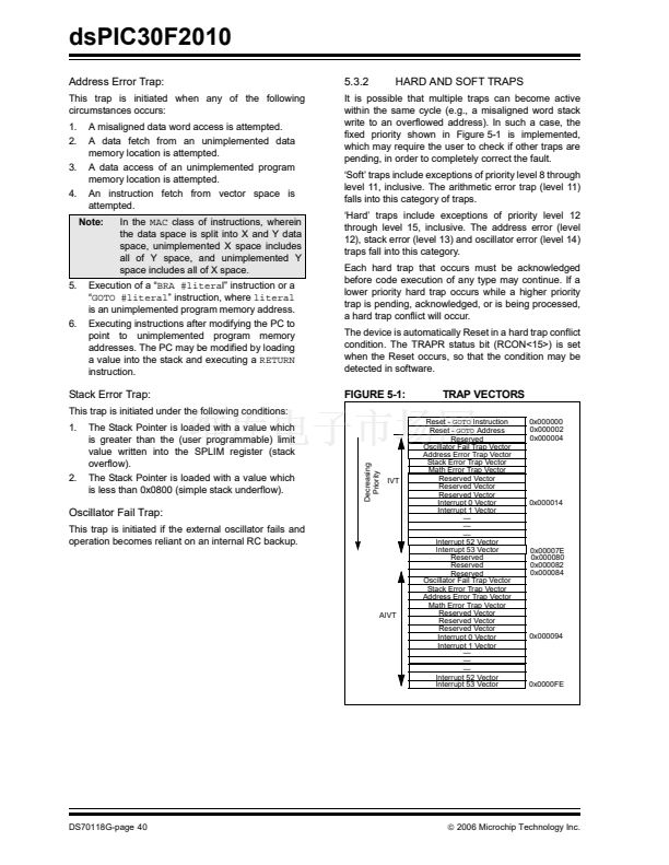
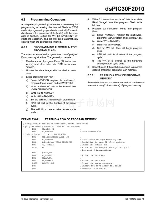
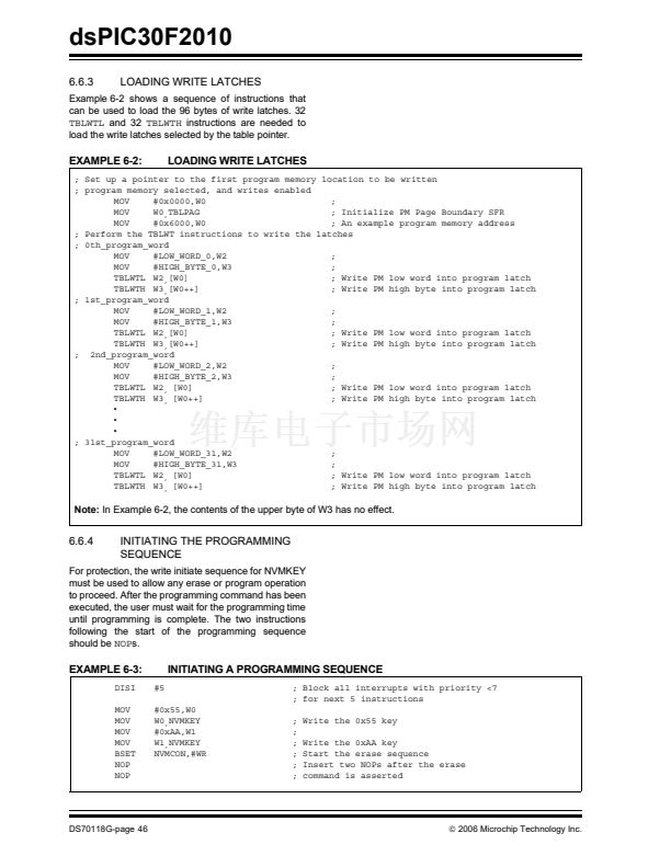
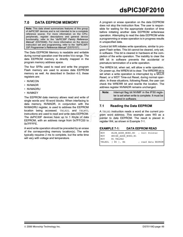
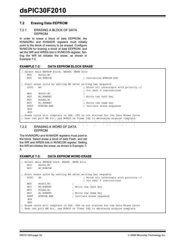
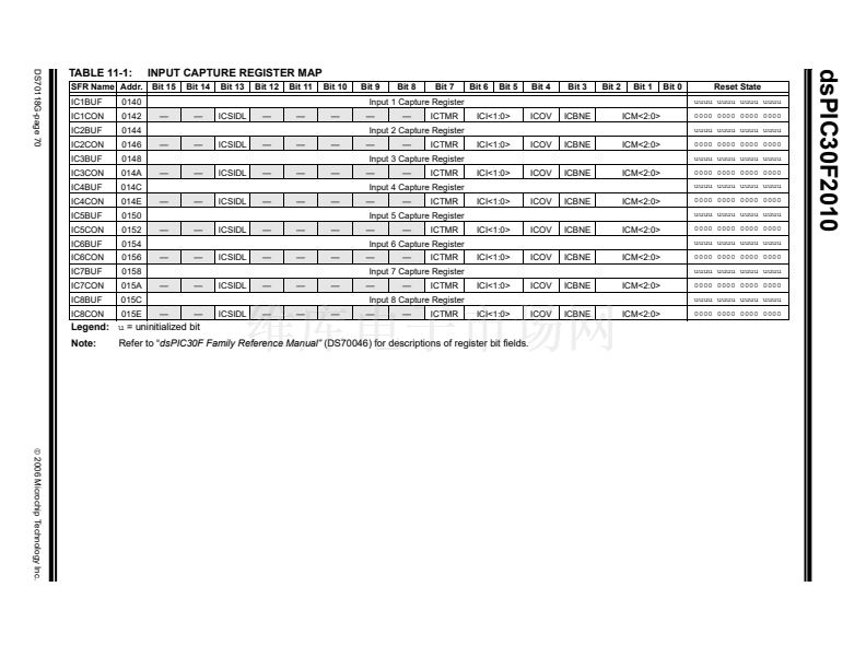
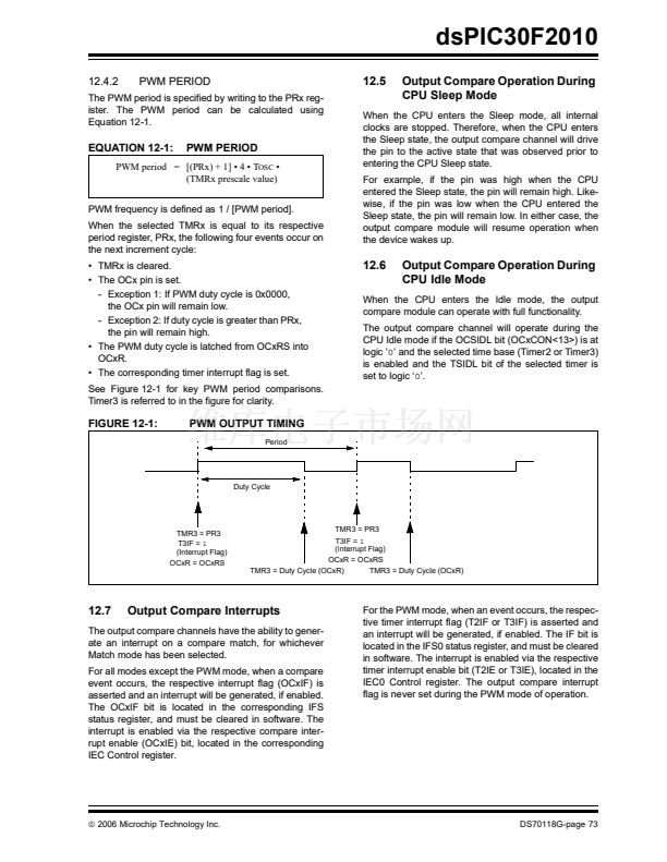
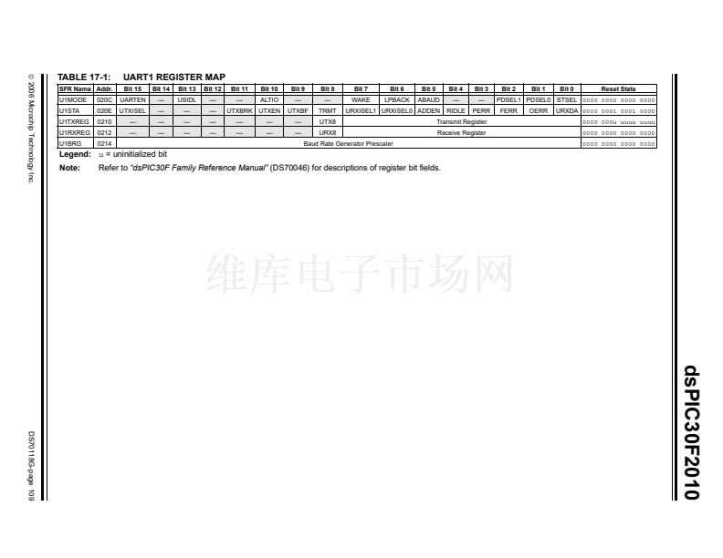
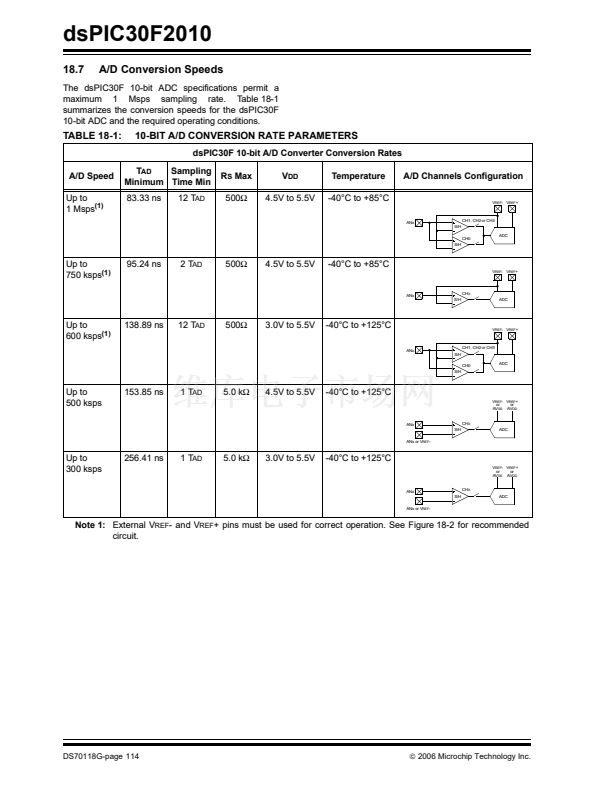
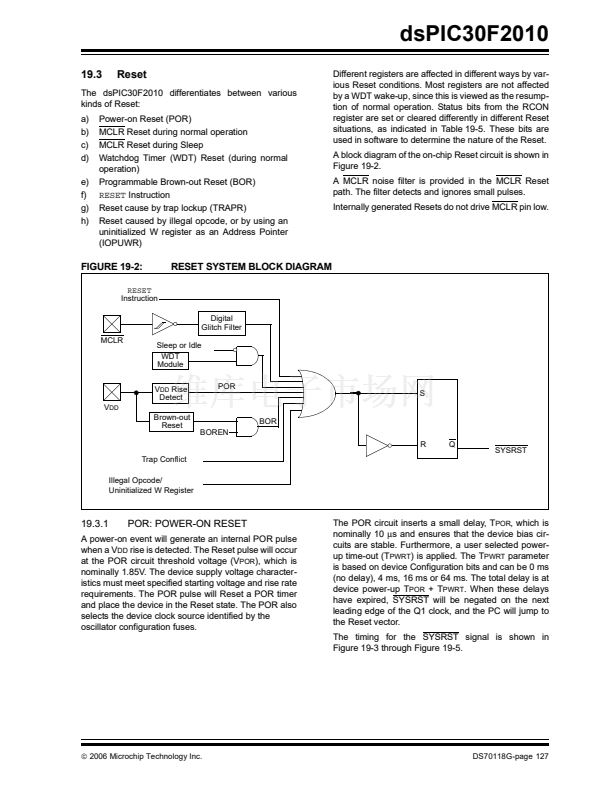
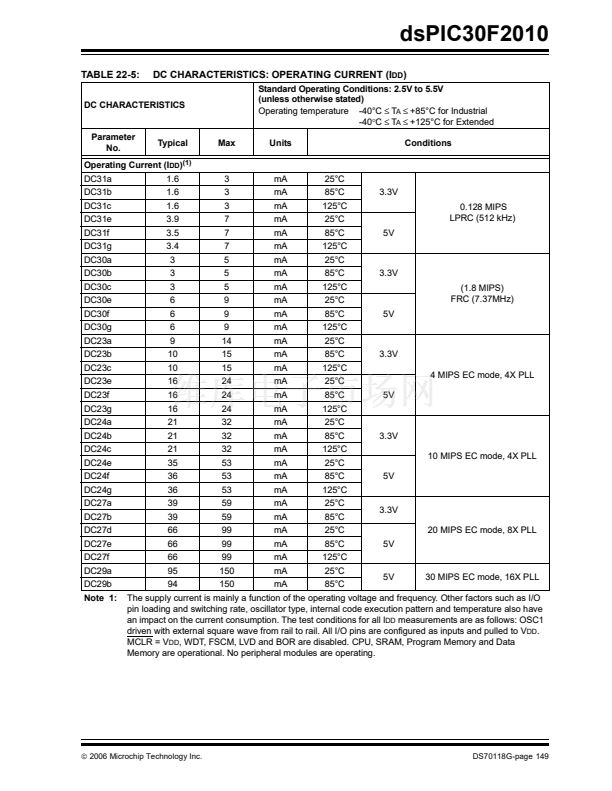
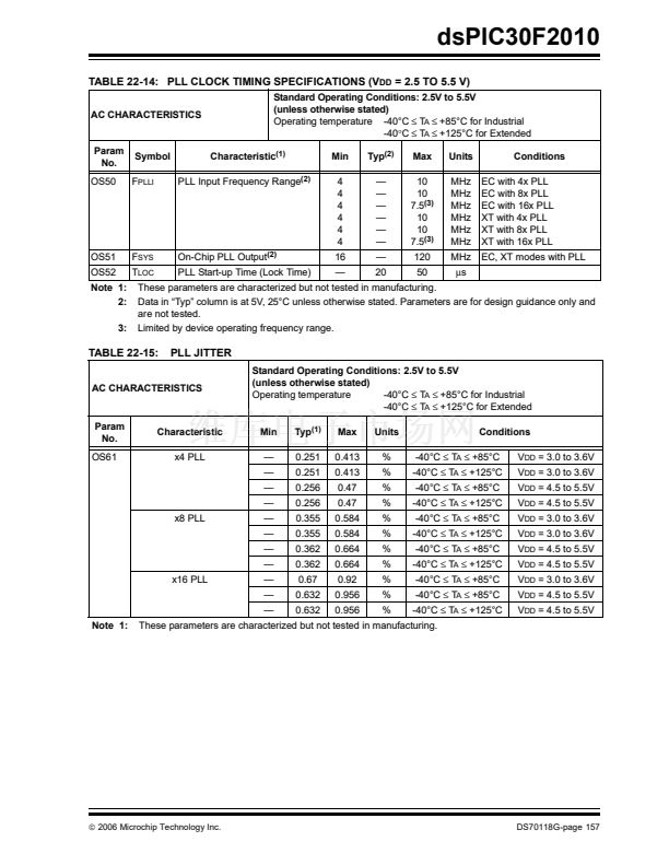
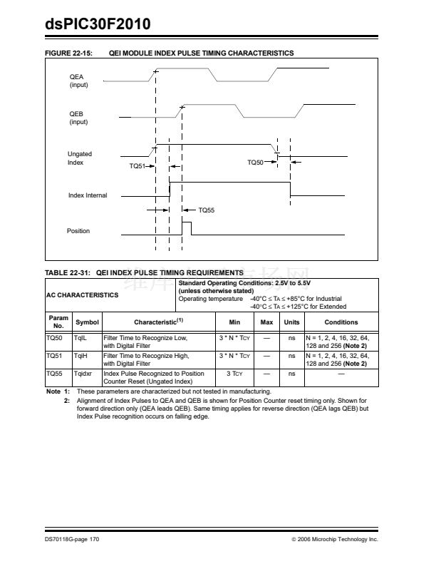
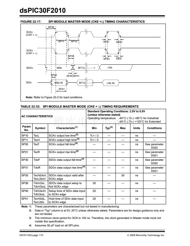
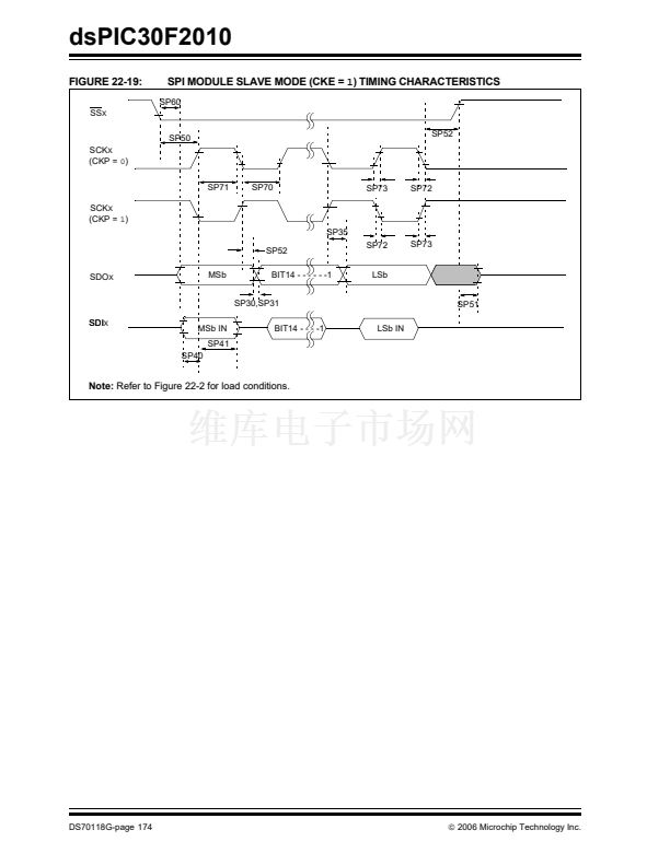
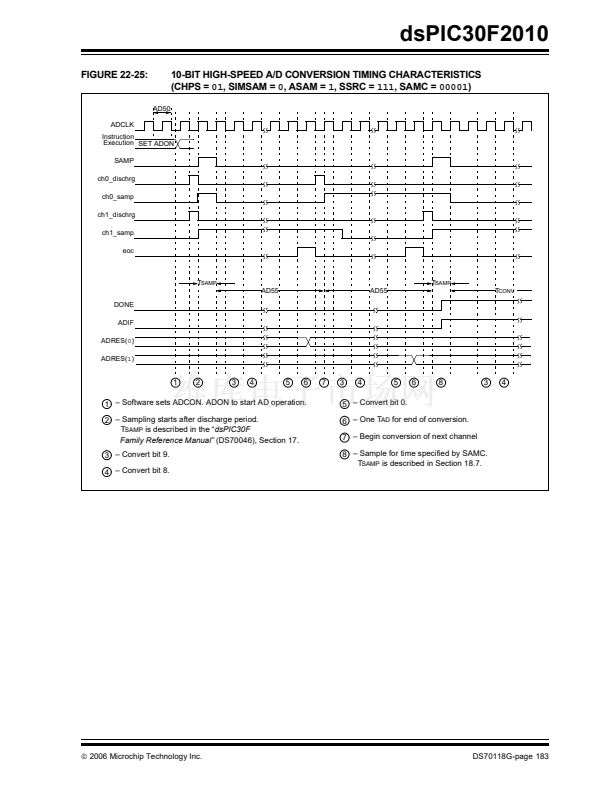
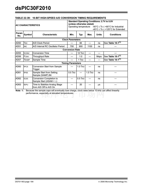
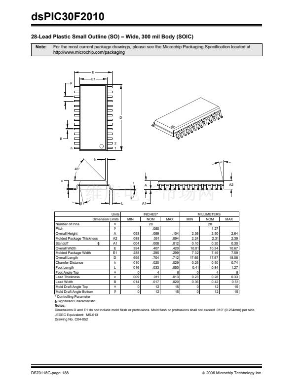
ister. The PWM period can be calculated using
Equation 12-1.
鈥?/div>
(TMRx prescale value)
PWM frequency is defined as 1 / [PWM period].
When the selected TMRx is equal to its respective
period register, PRx, the following four events occur on
the next increment cycle:
鈥?TMRx is cleared.
鈥?The OCx pin is set.
- Exception 1: If PWM duty cycle is 0x0000,
the OCx pin will remain low.
- Exception 2: If duty cycle is greater than PRx,
the pin will remain high.
鈥?The PWM duty cycle is latched from OCxRS into
OCxR.
鈥?The corresponding timer interrupt flag is set.
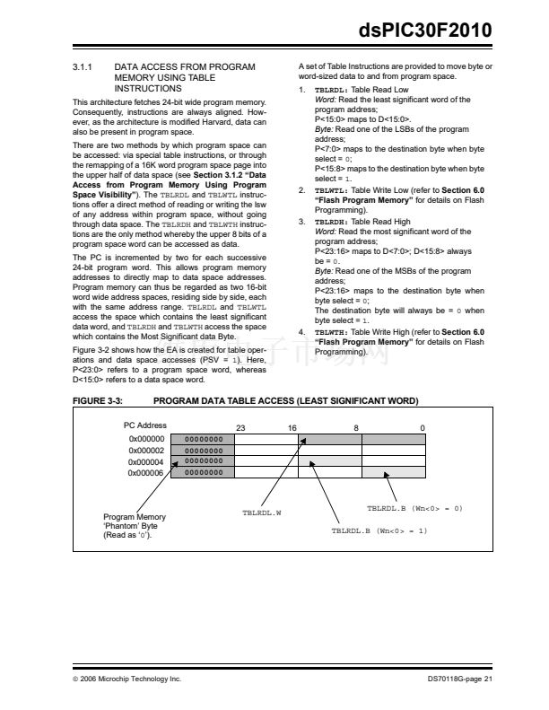
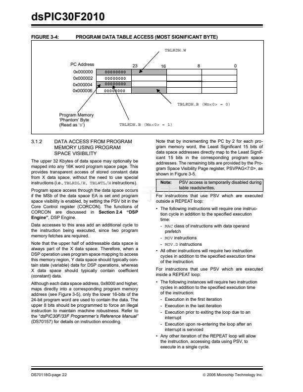
See Figure 12-1 for key PWM period comparisons.
Timer3 is referred to in the figure for clarity.
When the CPU enters the Sleep mode, all internal
clocks are stopped. Therefore, when the CPU enters
the Sleep state, the output compare channel will drive
the pin to the active state that was observed prior to
entering the CPU Sleep state.
For example, if the pin was high when the CPU
entered the Sleep state, the pin will remain high. Like-
wise, if the pin was low when the CPU entered the
Sleep state, the pin will remain low. In either case, the
output compare module will resume operation when
the device wakes up.
12.6
Output Compare Operation During
CPU Idle Mode
When the CPU enters the Idle mode, the output
compare module can operate with full functionality.
The output compare channel will operate during the
CPU Idle mode if the OCSIDL bit (OCxCON<13>) is at
logic 鈥?鈥?and the selected time base (Timer2 or Timer3)
is enabled and the TSIDL bit of the selected timer is
set to logic 鈥?鈥?
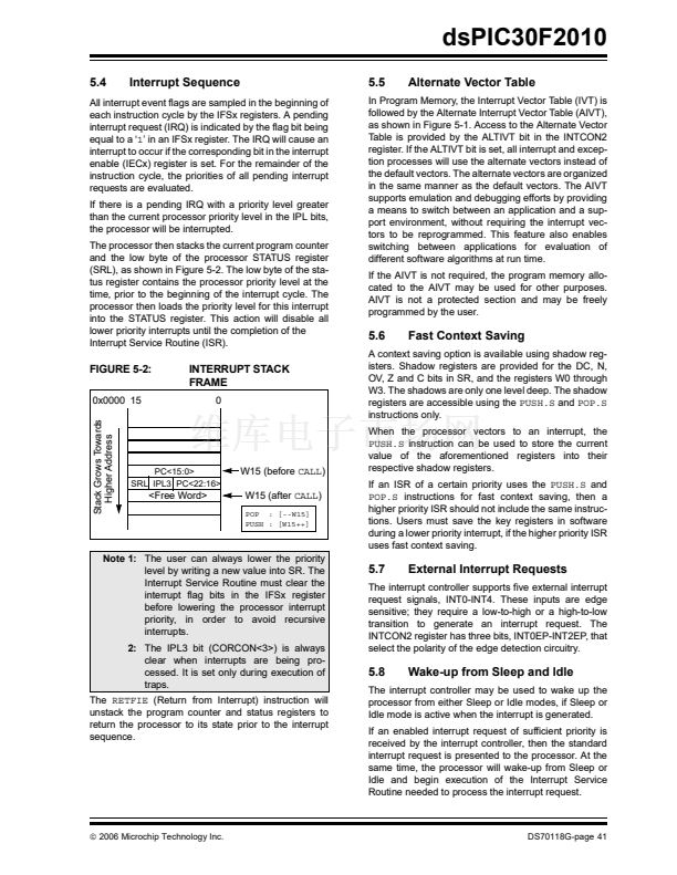
FIGURE 12-1:
PWM OUTPUT TIMING
Period
Duty Cycle
TMR3 = PR3
T3IF =
1
(Interrupt Flag)
OCxR = OCxRS
TMR3 = PR3
T3IF =
1
(Interrupt Flag)
OCxR = OCxRS
TMR3 = Duty Cycle (OCxR)
TMR3 = Duty Cycle (OCxR)
12.7
Output Compare Interrupts
The output compare channels have the ability to gener-
ate an interrupt on a compare match, for whichever
Match mode has been selected.
For all modes except the PWM mode, when a compare
event occurs, the respective interrupt flag (OCxIF) is
asserted and an interrupt will be generated, if enabled.
The OCxIF bit is located in the corresponding IFS
status register, and must be cleared in software. The
interrupt is enabled via the respective compare inter-
rupt enable (OCxIE) bit, located in the corresponding
IEC Control register.
For the PWM mode, when an event occurs, the respec-
tive timer interrupt flag (T2IF or T3IF) is asserted and
an interrupt will be generated, if enabled. The IF bit is
located in the IFS0 status register, and must be cleared
in software. The interrupt is enabled via the respective
timer interrupt enable bit (T2IE or T3IE), located in the
IEC0 Control register. The output compare interrupt
flag is never set during the PWM mode of operation.
漏
2006 Microchip Technology Inc.
DS70118G-page 73


 1
1
 2
2
 3
3
 4
4
 5
5
 6
6
 7
7
 8
8
 9
9
 10
10
 11
11
 12
12
 13
13
 14
14
 15
15
 16
16
 17
17
 18
18
 19
19
 20
20
 21
21
 22
22
 23
23
 24
24
 25
25
 26
26
 27
27
 28
28
 29
29
 30
30
 31
31
 32
32
 33
33
 34
34
 35
35
 36
36
 37
37
 38
38
 39
39
 40
40
 41
41
 42
42
 43
43
 44
44
 45
45
 46
46
 47
47
 48
48
 49
49
 50
50
 51
51
 52
52
 53
53
 54
54
 55
55
 56
56
 57
57
 58
58
 59
59
 60
60
 61
61
 62
62
 63
63
 64
64
 65
65
 66
66
 67
67
 68
68
 69
69
 70
70
 71
71
 72
72
 73
73
 74
74
 75
75
 76
76
 77
77
 78
78
 79
79
 80
80
 81
81
 82
82
 83
83
 84
84
 85
85
 86
86
 87
87
 88
88
 89
89
 90
90
 91
91
 92
92
 93
93
 94
94
 95
95
 96
96
 97
97
 98
98
 99
99
 100
100
 101
101
 102
102
 103
103
 104
104
 105
105
 106
106
 107
107
 108
108
 109
109
 110
110
 111
111
 112
112
 113
113
 114
114
 115
115
 116
116
 117
117
 118
118
 119
119
 120
120
 121
121
 122
122
 123
123
 124
124
 125
125
 126
126
 127
127
 128
128
 129
129
 130
130
 131
131
 132
132
 133
133
 134
134
 135
135
 136
136
 137
137
 138
138
 139
139
 140
140
 141
141
 142
142
 143
143
 144
144
 145
145
 146
146
 147
147
 148
148
 149
149
 150
150
 151
151
 152
152
 153
153
 154
154
 155
155
 156
156
 157
157
 158
158
 159
159
 160
160
 161
161
 162
162
 163
163
 164
164
 165
165
 166
166
 167
167
 168
168
 169
169
 170
170
 171
171
 172
172
 173
173
 174
174
 175
175
 176
176
 177
177
 178
178
 179
179
 180
180
 181
181
 182
182
 183
183
 184
184
 185
185
 186
186
 187
187
 188
188
 189
189
 190
190
 191
191
 192
192
 193
193
 194
194
 195
195
 196
196
 197
197
 198
198
 199
199
 200
200
 201
201
 202
202
 203
203
