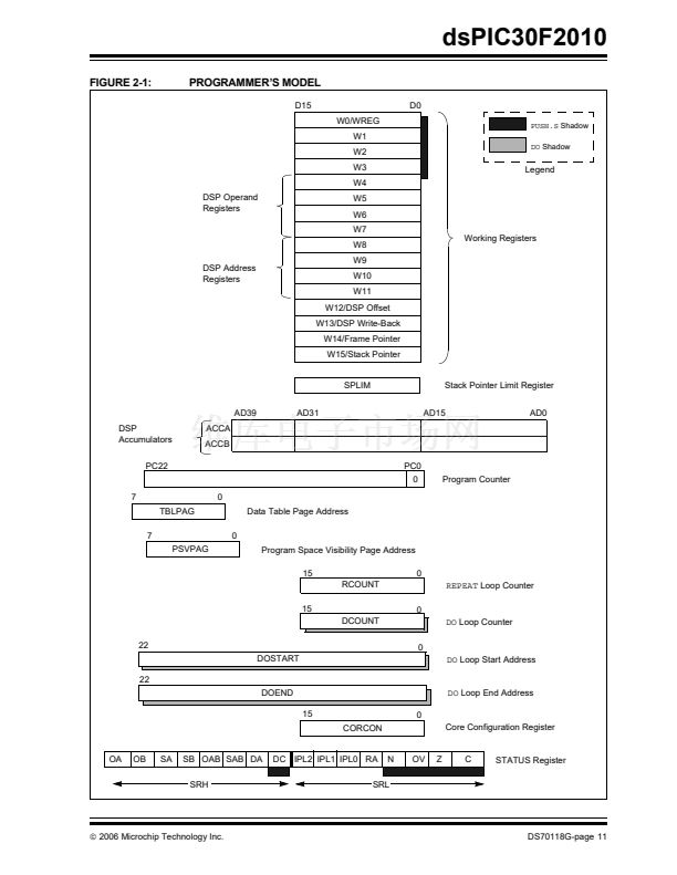
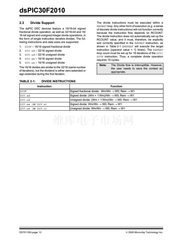
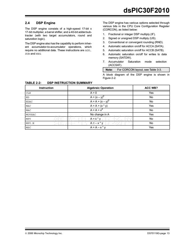
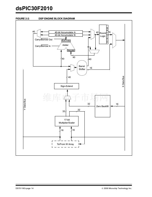
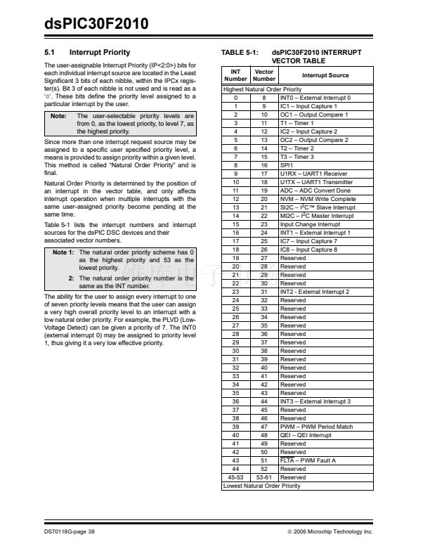
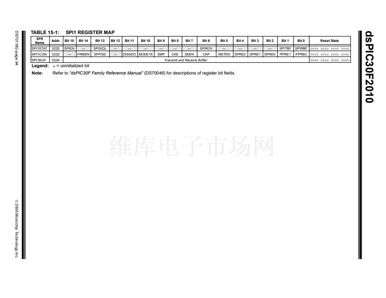
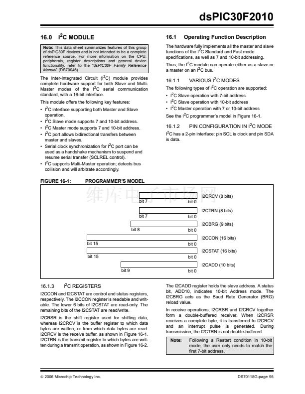
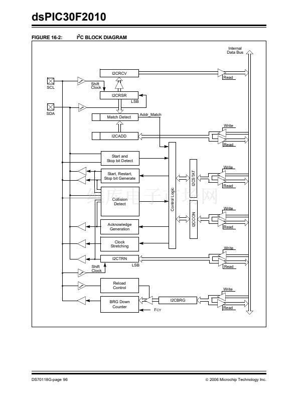
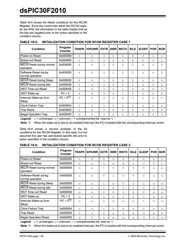
鈥?/div>
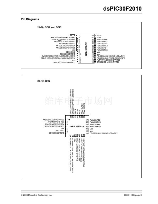
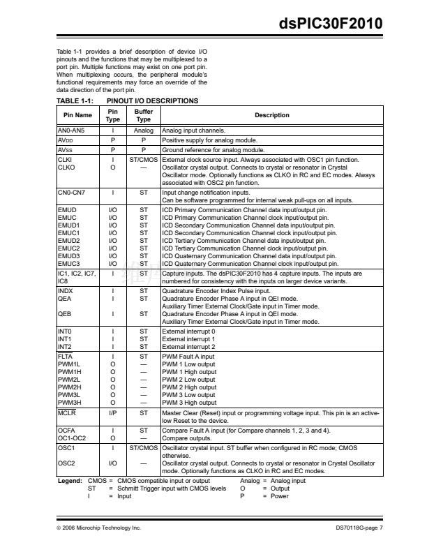
Input change notification inputs.
Can be software programmed for internal weak pull-ups on all inputs.
ICD Primary Communication Channel data input/output pin.
ICD Primary Communication Channel clock input/output pin.
ICD Secondary Communication Channel data input/output pin.
ICD Secondary Communication Channel clock input/output pin.
ICD Tertiary Communication Channel data input/output pin.
ICD Tertiary Communication Channel clock input/output pin.
ICD Quaternary Communication Channel data input/output pin.
ICD Quaternary Communication Channel clock input/output pin.
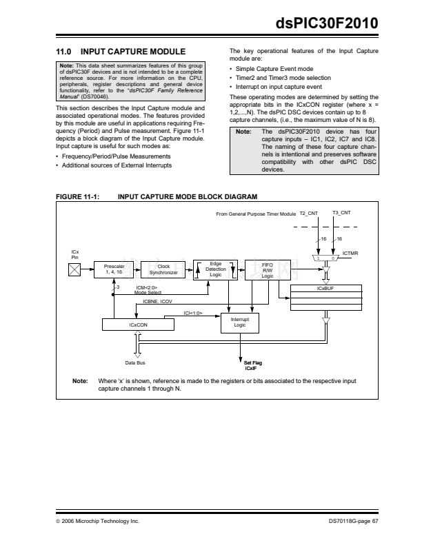
Capture inputs. The dsPIC30F2010 has 4 capture inputs. The inputs are
numbered for consistency with the inputs on larger device variants.
Quadrature Encoder Index Pulse input.
Quadrature Encoder Phase A input in QEI mode.
Auxiliary Timer External Clock/Gate input in Timer mode.
Quadrature Encoder Phase A input in QEI mode.
Auxiliary Timer External Clock/Gate input in Timer mode.
External interrupt 0
External interrupt 1
External interrupt 2
PWM Fault A input
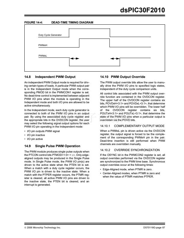
PWM 1 Low output
PWM 1 High output
PWM 2 Low output
PWM 2 High output
PWM 3 Low output
PWM 3 High output
Master Clear (Reset) input or programming voltage input. This pin is an active-
low Reset to the device.
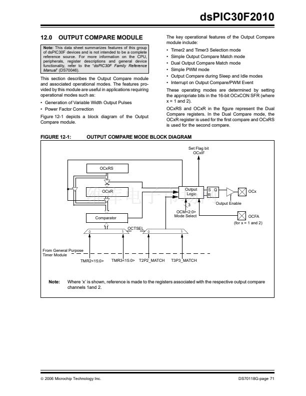
Compare Fault A input (for Compare channels 1, 2, 3 and 4).
Compare outputs.
CN0-CN7
EMUD
EMUC
EMUD1
EMUC1
EMUD2
EMUC2
EMUD3
EMUC3
IC1, IC2, IC7,
IC8
INDX
QEA
QEB
INT0
INT1
INT2
FLTA
PWM1L
PWM1H
PWM2L
PWM2H
PWM3L
PWM3H
MCLR
OCFA
OC1-OC2
OSC1
OSC2
I
I/O
I/O
I/O
I/O
I/O
I/O
I/O
I/O
I
I
I
I
I
I
I
I
O
O
O
O
O
O
I/P
I
O
I
I/O
ST/CMOS Oscillator crystal input. ST buffer when configured in RC mode; CMOS
otherwise.
鈥?/div>
Oscillator crystal output. Connects to crystal or resonator in Crystal Oscillator
mode. Optionally functions as CLKO in RC and EC modes.
Analog = Analog input
O
= Output
P
= Power
Legend:
CMOS = CMOS compatible input or output
ST
= Schmitt Trigger input with CMOS levels
I
= Input
漏
2006 Microchip Technology Inc.
DS70118G-page 7


 1
1
 2
2
 3
3
 4
4
 5
5
 6
6
 7
7
 8
8
 9
9
 10
10
 11
11
 12
12
 13
13
 14
14
 15
15
 16
16
 17
17
 18
18
 19
19
 20
20
 21
21
 22
22
 23
23
 24
24
 25
25
 26
26
 27
27
 28
28
 29
29
 30
30
 31
31
 32
32
 33
33
 34
34
 35
35
 36
36
 37
37
 38
38
 39
39
 40
40
 41
41
 42
42
 43
43
 44
44
 45
45
 46
46
 47
47
 48
48
 49
49
 50
50
 51
51
 52
52
 53
53
 54
54
 55
55
 56
56
 57
57
 58
58
 59
59
 60
60
 61
61
 62
62
 63
63
 64
64
 65
65
 66
66
 67
67
 68
68
 69
69
 70
70
 71
71
 72
72
 73
73
 74
74
 75
75
 76
76
 77
77
 78
78
 79
79
 80
80
 81
81
 82
82
 83
83
 84
84
 85
85
 86
86
 87
87
 88
88
 89
89
 90
90
 91
91
 92
92
 93
93
 94
94
 95
95
 96
96
 97
97
 98
98
 99
99
 100
100
 101
101
 102
102
 103
103
 104
104
 105
105
 106
106
 107
107
 108
108
 109
109
 110
110
 111
111
 112
112
 113
113
 114
114
 115
115
 116
116
 117
117
 118
118
 119
119
 120
120
 121
121
 122
122
 123
123
 124
124
 125
125
 126
126
 127
127
 128
128
 129
129
 130
130
 131
131
 132
132
 133
133
 134
134
 135
135
 136
136
 137
137
 138
138
 139
139
 140
140
 141
141
 142
142
 143
143
 144
144
 145
145
 146
146
 147
147
 148
148
 149
149
 150
150
 151
151
 152
152
 153
153
 154
154
 155
155
 156
156
 157
157
 158
158
 159
159
 160
160
 161
161
 162
162
 163
163
 164
164
 165
165
 166
166
 167
167
 168
168
 169
169
 170
170
 171
171
 172
172
 173
173
 174
174
 175
175
 176
176
 177
177
 178
178
 179
179
 180
180
 181
181
 182
182
 183
183
 184
184
 185
185
 186
186
 187
187
 188
188
 189
189
 190
190
 191
191
 192
192
 193
193
 194
194
 195
195
 196
196
 197
197
 198
198
 199
199
 200
200
 201
201
 202
202
 203
203
