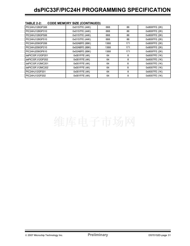
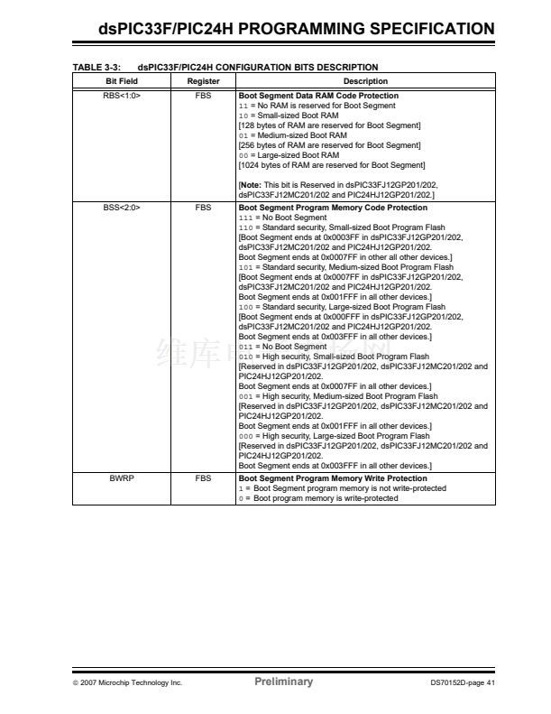
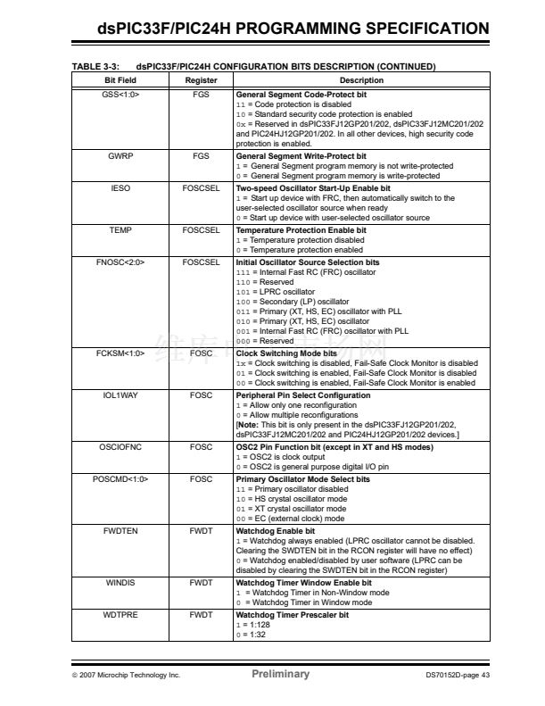
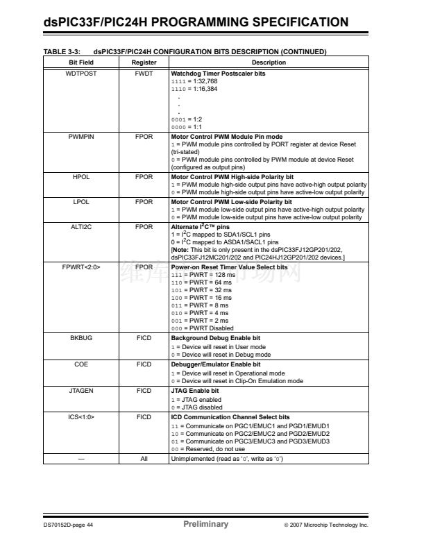
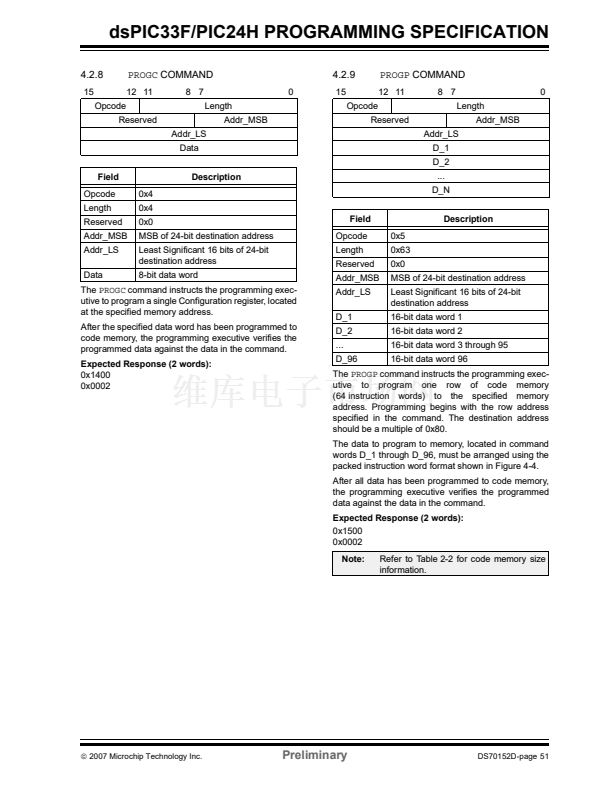
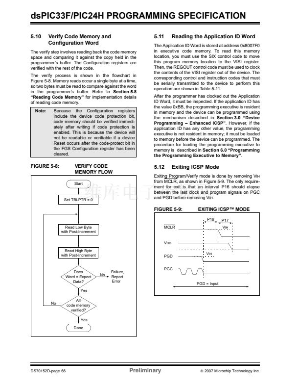
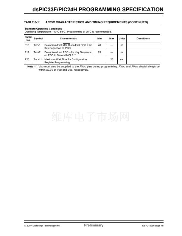
1101 0100 0011 0100 1000 0101 0001鈥?/div>
(more easily remembered as 0x4D434851 in hexa-
decimal). The device will enter Program/Verify mode only
if the sequence is valid. The Most Significant bit (MSb) of
the most significant nibble must be shifted in first.
Once the key sequence is complete, V
IH
must be
applied to MCLR and held at that level for as long as
Program/Verify mode is to be maintained. An interval of
at least time P19 and P7 must elapse before presenting
data on PGD. Signals appearing on PGD before P7
has elapsed will not be interpreted as valid.
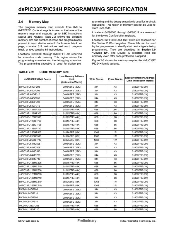
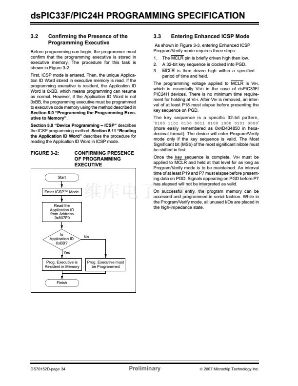
On successful entry, the program memory can be
accessed and programmed in serial fashion. While
in ICSP mode, all unused I/Os are placed in the
high-impedance state.
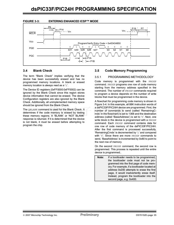
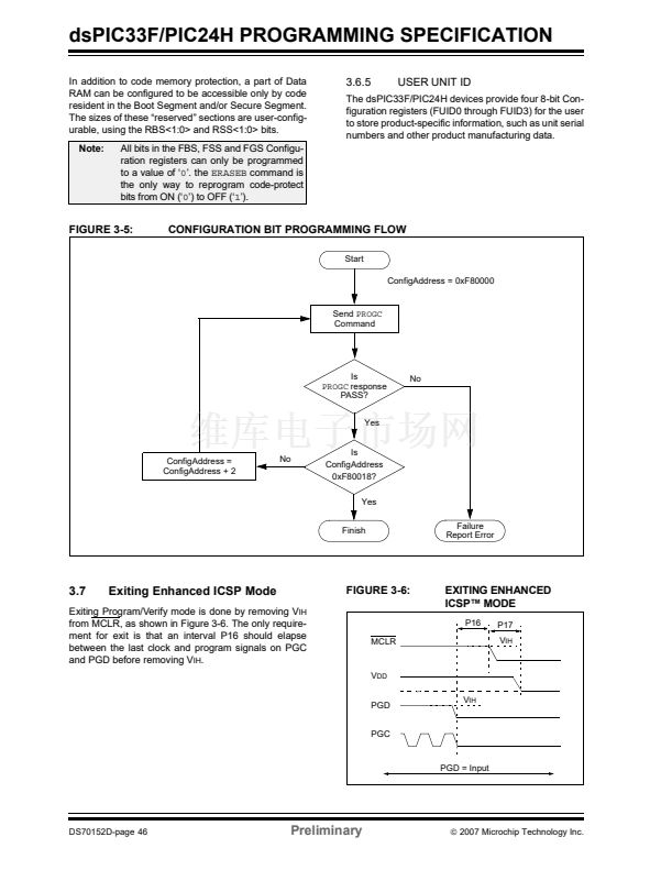
As shown in Figure 5-4, entering ICSP Program/Verify
mode requires three steps:
1.
2.
3.
MCLR is briefly driven high then low.
A 32-bit key sequence is clocked into PGD.
MCLR is then driven high within a specified
period of time and held.
The programming voltage applied to MCLR is V
IH
,
which is essentially V
DD
in the case of dsPIC33F/
PIC24H devices. There is no minimum time require-
ment for holding at V
IH
. After V
IH
is removed, an inter-
val of at least P18 must elapse before presenting the
key sequence on PGD.
FIGURE 5-4:
ENTERING ICSP鈩?MODE
P6
P14
P19
V
IH
V
IH
P7
MCLR
V
DD
PGD
0
b31
Program/Verify Entry Code = 0x4D434851
1
b30
0
b29
0
b28
1
b27
...
0
b3
0
b2
0
b1
1
b0
PGC
P18
P1A
P1B
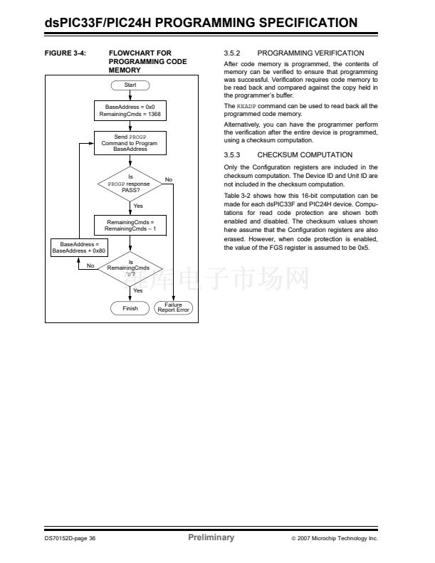
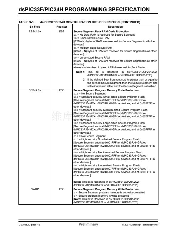
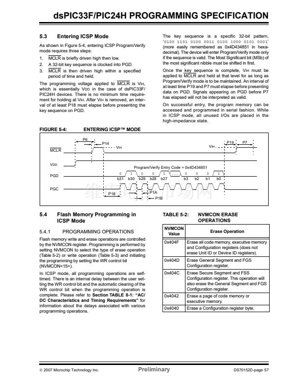
5.4
5.4.1
Flash Memory Programming in
ICSP Mode
PROGRAMMING OPERATIONS
TABLE 5-2:
NVMCON
Value
0x404F
NVMCON ERASE
OPERATIONS
Erase Operation
Flash memory write and erase operations are controlled
by the NVMCON register. Programming is performed by
setting NVMCON to select the type of erase operation
(Table 5-2) or write operation (Table 5-3) and initiating
the programming by setting the WR control bit
(NVMCON<15>).
In ICSP mode, all programming operations are self-
timed. There is an internal delay between the user set-
ting the WR control bit and the automatic clearing of the
WR control bit when the programming operation is
complete. Please refer to
Section TABLE 8-1: 鈥淎C/
DC Characteristics and Timing Requirements鈥?/span>
for
information about the delays associated with various
programming operations.
Erase all code memory, executive memory
and Configuration registers (does not
erase Unit ID or Device ID registers).
Erase General Segment and FGS
Configuration register.
Erase Secure Segment and FSS
Configuration register. This operation will
also erase the General Segment and FGS
Configuration register.
Erase a page of code memory or
executive memory.
Erase a Configuration register byte.
0x404D
0x404C
0x4042
0x4040
漏
2007 Microchip Technology Inc.
Preliminary
DS70152D-page 57


 1
1
 2
2
 3
3
 4
4
 5
5
 6
6
 7
7
 8
8
 9
9
 10
10
 11
11
 12
12
 13
13
 14
14
 15
15
 16
16
 17
17
 18
18
 19
19
 20
20
 21
21
 22
22
 23
23
 24
24
 25
25
 26
26
 27
27
 28
28
 29
29
 30
30
 31
31
 32
32
 33
33
 34
34
 35
35
 36
36
 37
37
 38
38
 39
39
 40
40
 41
41
 42
42
 43
43
 44
44
 45
45
 46
46
 47
47
 48
48
 49
49
 50
50
 51
51
 52
52
 53
53
 54
54
 55
55
 56
56
 57
57
 58
58
 59
59
 60
60
 61
61
 62
62
 63
63
 64
64
 65
65
 66
66
 67
67
 68
68
 69
69
 70
70
 71
71
 72
72
 73
73
 74
74
 75
75
 76
76
 77
77
 78
78
 79
79
 80
80
