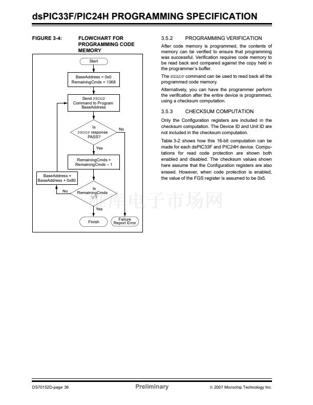
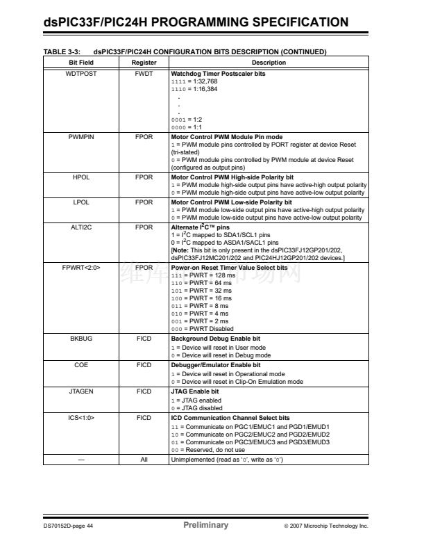
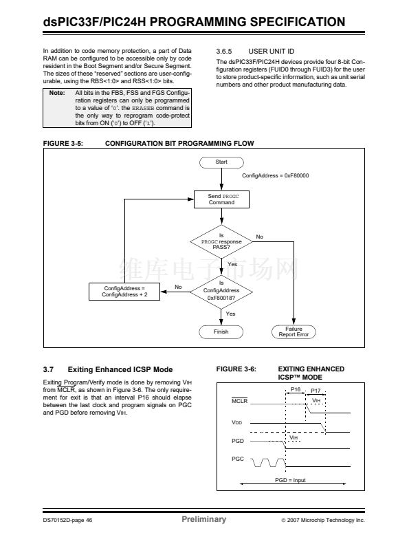
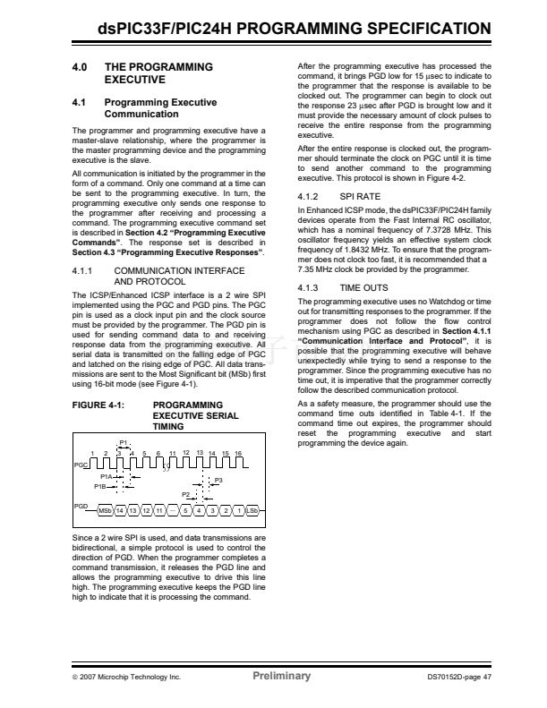
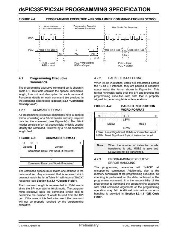
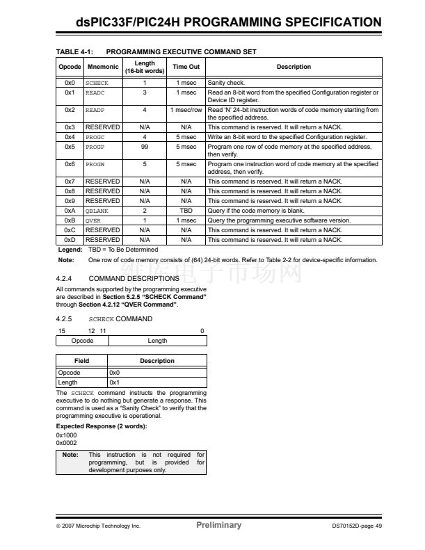
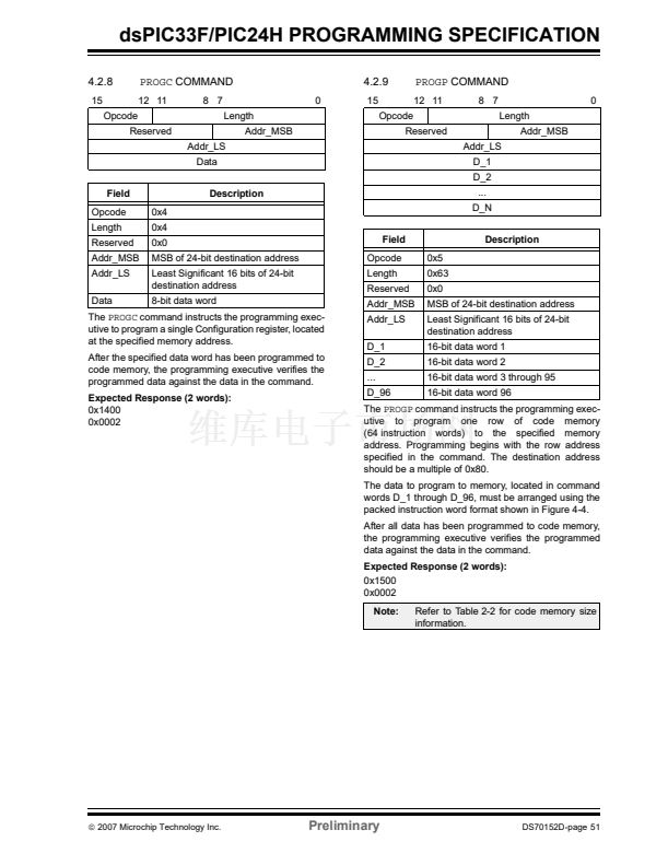
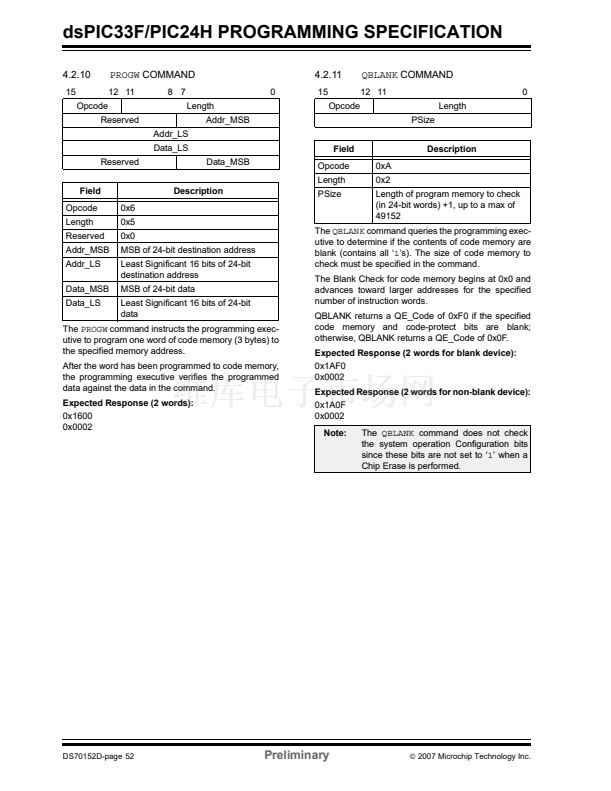
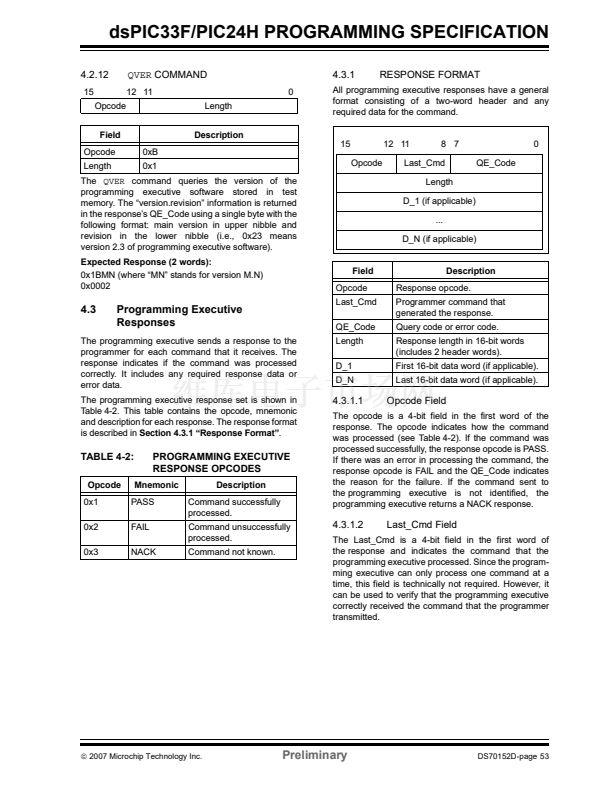
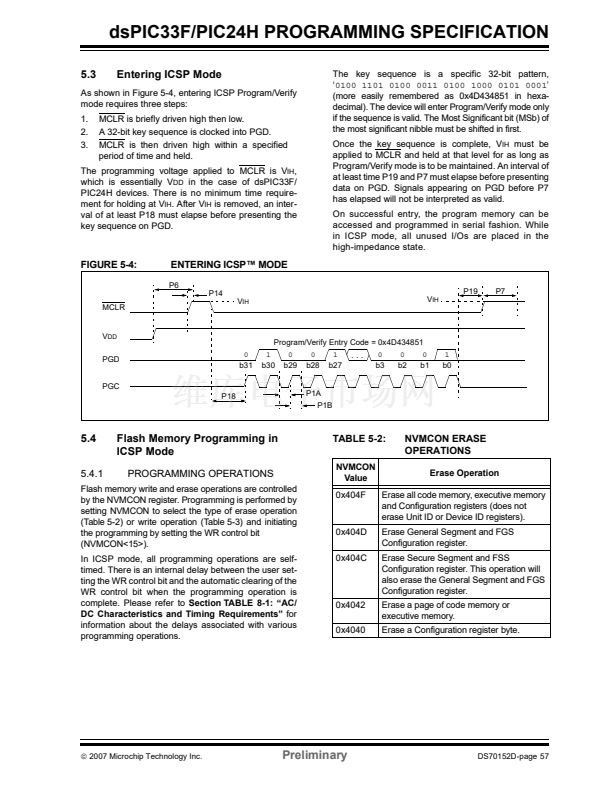
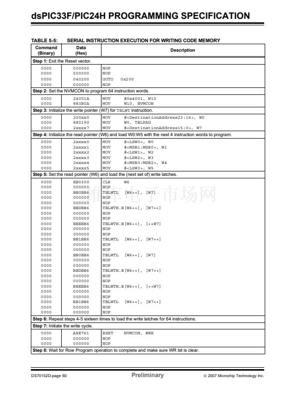
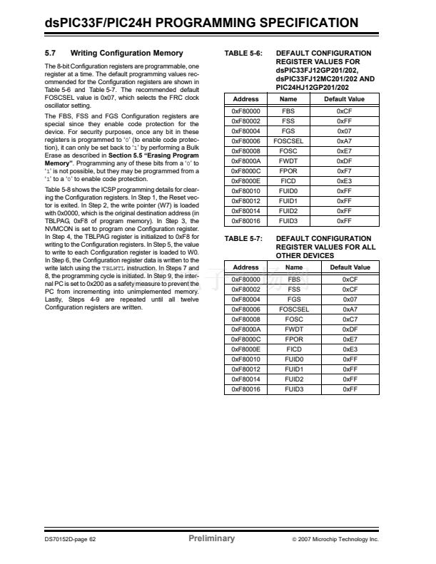
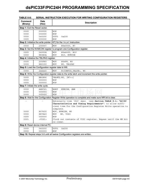
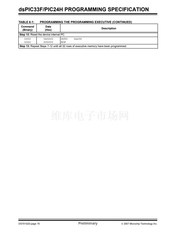
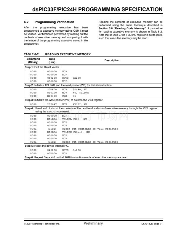
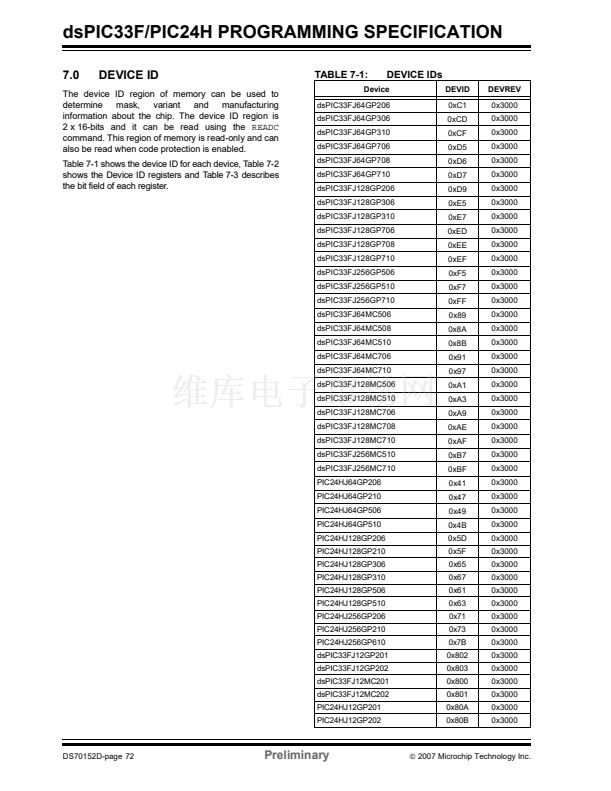
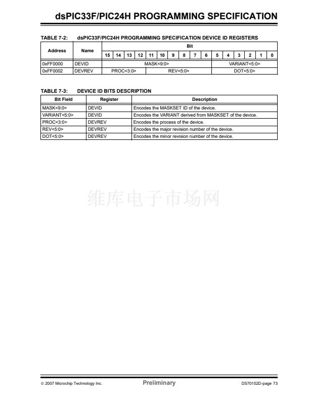
dsPIC33F/PIC24H PROGRAMMING SPECIFICATION
8.0
AC/DC CHARACTERISTICS
AND TIMING REQUIREMENTS
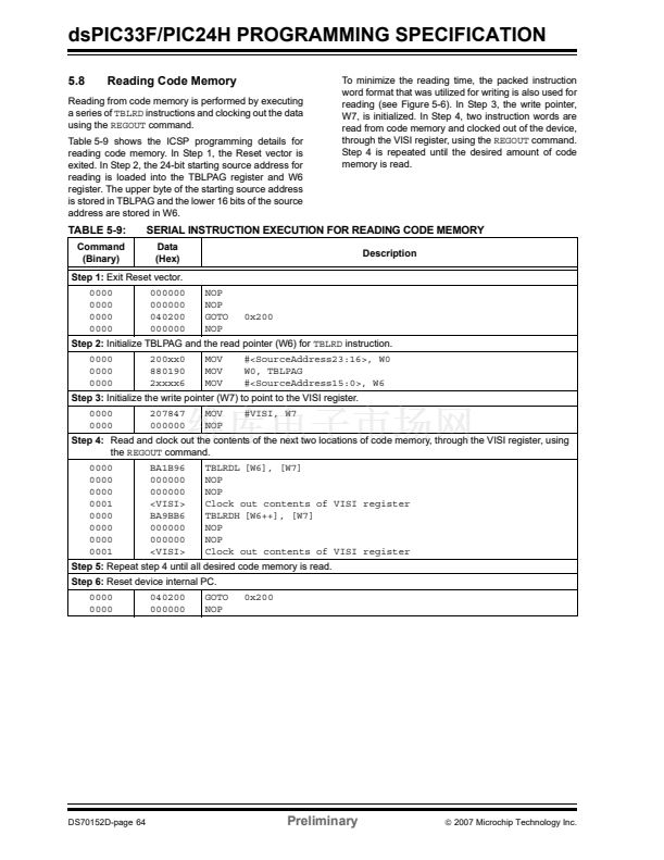
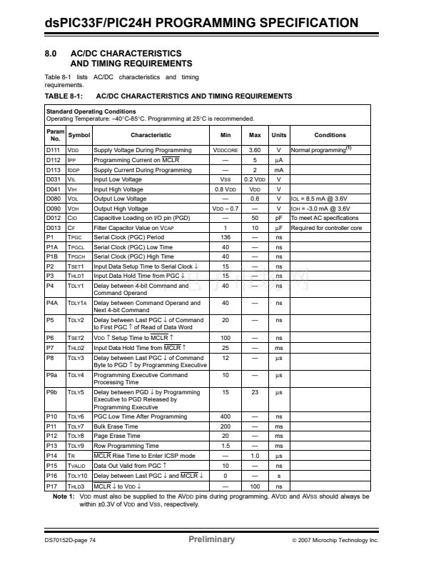
Table 8-1 lists AC/DC characteristics and timing
requirements.
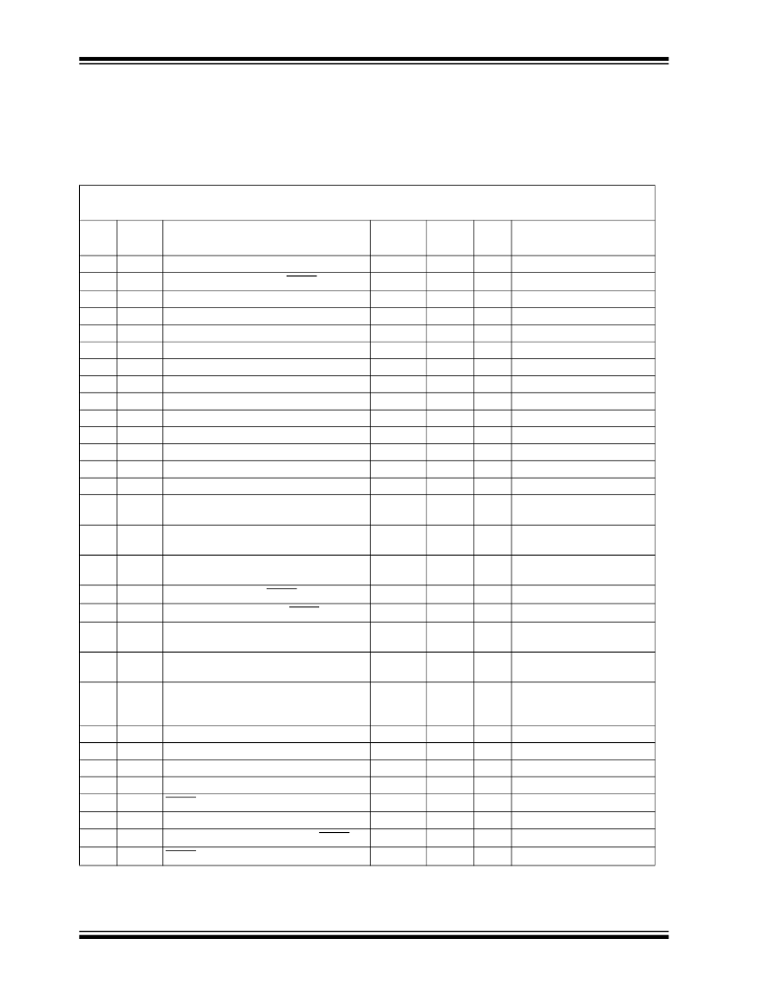
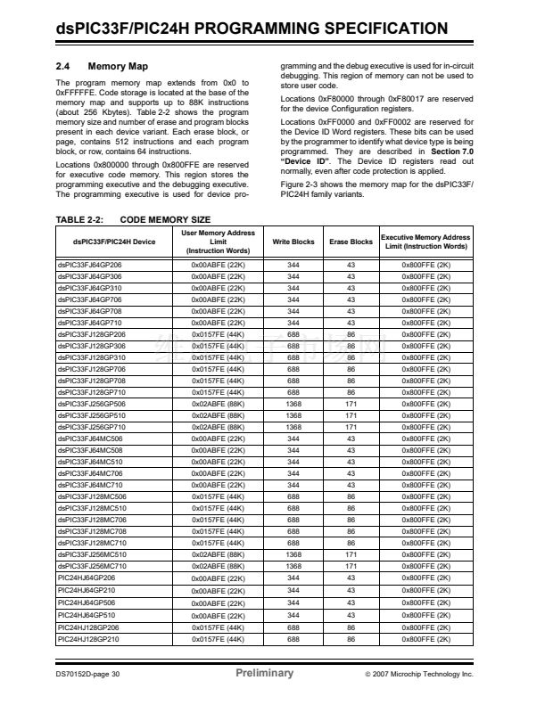
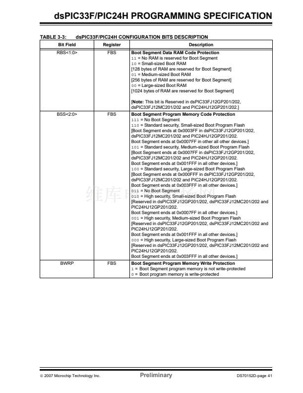
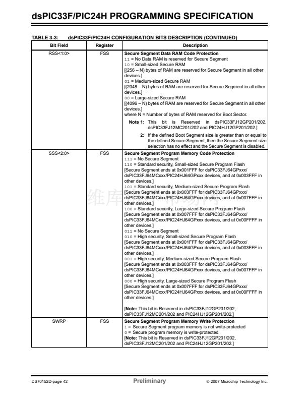
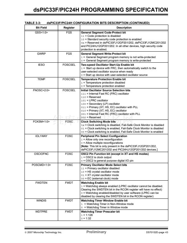
TABLE 8-1:
AC/DC CHARACTERISTICS AND TIMING REQUIREMENTS
Standard Operating Conditions
Operating Temperature: 鈥?0掳C-85掳C. Programming at 25掳C is recommended.
Param
Symbol
No.
D111
D112
D113
D031
D041
D080
D090
D012
D013
P1
P1A
P1B
P2
P3
P4
P4A
P5
P6
P7
P8
P9a
P9b
V
DD
I
PP
I
DDP
V
IL
V
IH
V
OL
V
OH
C
IO
C
F
T
PGC
T
PGCL
T
PGCH
T
SET
1
T
HLD
1
T
DLY
1
T
DLY
1
A
T
DLY
2
T
SET
2
T
HLD
2
T
DLY
3
T
DLY
4
T
DLY
5
Characteristic
Supply Voltage During Programming
Programming Current on MCLR
Supply Current During Programming
Input Low Voltage
Input High Voltage
Output Low Voltage
Output High Voltage
Capacitive Loading on I/O pin (PGD)
Filter Capacitor Value on V
CAP
Serial Clock (PGC) Period
Serial Clock (PGC) Low Time
Serial Clock (PGC) High Time
Input Data Setup Time to Serial Clock
鈫?/div>
Input Data Hold Time from PGC
鈫?/div>
Delay between 4-bit Command and
Command Operand
Delay between Command Operand and
Next 4-bit Command
Delay between Last PGC
鈫?/div>
of Command
to First PGC
鈫?/div>
of Read of Data Word
V
DD
鈫?/div>
Setup Time to MCLR
鈫?/div>
Input Data Hold Time from MCLR
鈫?/div>
Delay between Last PGC
鈫?/div>
of Command
Byte to PGD
鈫?/div>
by Programming Executive
Programming Executive Command
Processing Time
Delay between PGD
鈫?/div>
by Programming
Executive to PGD Released by
Programming Executive
PGC Low Time After Programming
Bulk Erase Time
Page Erase Time
Row Programming Time
MCLR Rise Time to Enter ICSP mode
Data Out Valid from PGC
鈫?/div>
Delay between Last PGC
鈫?/div>
and MCLR
鈫?/div>
MCLR
鈫?/div>
to V
DD
鈫?/div>
Min
V
DDCORE
鈥?/div>
鈥?/div>
V
SS
0.8 V
DD
鈥?/div>
V
DD
鈥?0.7
鈥?/div>
1
136
40
40
15
15
40
40
20
100
25
12
10
15
Max
3.60
5
2
0.2 V
DD
V
DD
0.6
鈥?/div>
50
10
鈥?/div>
鈥?/div>
鈥?/div>
鈥?/div>
鈥?/div>
鈥?/div>
鈥?/div>
鈥?/div>
鈥?/div>
鈥?/div>
鈥?/div>
鈥?/div>
23
Units
V
渭A
mA
V
V
V
V
pF
渭F
ns
ns
ns
ns
ns
ns
ns
ns
ns
ms
渭s
渭s
渭s
I
OL
= 8.5 mA @ 3.6V
I
OH
= -3.0 mA @ 3.6V
To meet AC specifications
Required for controller core
Conditions
Normal programming
(1)
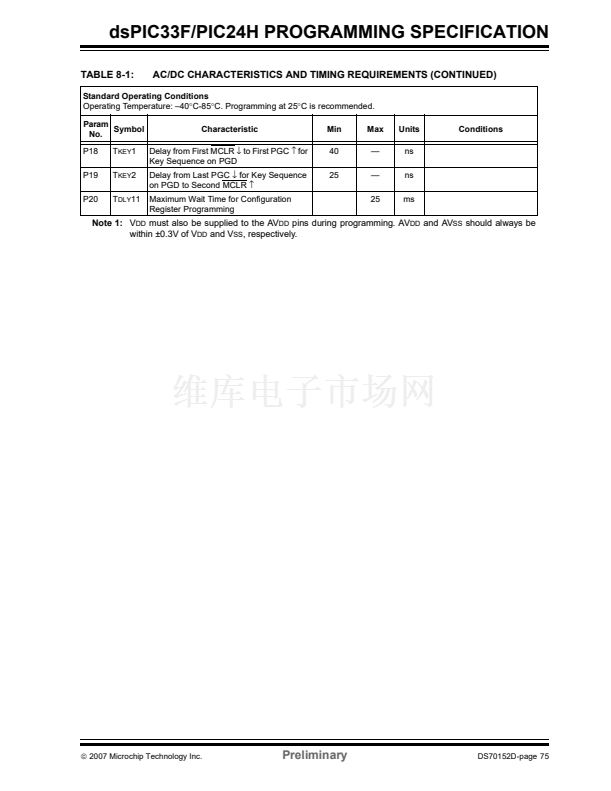
P10
P11
P12
P13
P14
P15
P16
P17
T
DLY
6
T
DLY
7
T
DLY
8
T
DLY
9
T
R
T
VALID
T
DLY
10
T
HLD
3
400
200
20
1.5
鈥?/div>
10
0
鈥?/div>
鈥?/div>
鈥?/div>
鈥?/div>
鈥?/div>
1.0
鈥?/div>
鈥?/div>
100
ns
ms
ms
ms
渭s
ns
s
ns
Note 1:
V
DD
must also be supplied to the AV
DD
pins during programming. AV
DD
and AV
SS
should always be
within 卤0.3V of V
DD
and V
SS
, respectively.
DS70152D-page 74
Preliminary
漏
2007 Microchip Technology Inc.
dsPIC33FJ128MC510相关型号PDF文件下载
-
型号
版本
描述
厂商
下载
-
英文版
Serial Peripheral Interface - Master/Slave
DCD
-
英文版
Serial Peripheral Interface - Slave
DCD
-
英文版
Flash Programming Specification
-
英文版
Flash Programming Specification
MICROCHIP ...
-
英文版
dsPIC High-Performance 16-bit Digital Signal Controller Fami...
-
英文版
dsPIC High-Performance 16-bit Digital Signal Controller Fami...
MICROCHIP ...
-
英文版
High-Performance, 16-bit Digital Signal Controllers
-
英文版
Serial Peripheral Interface Master/Slave with FIFO
DCD [Digit...
-
英文版
28/44-Pin High-Performance Switch Mode Power Supply Digital ...
-
英文版
28/44-Pin High-Performance Switch Mode Power Supply Digital ...
MICROCHIP ...
-
英文版
-
英文版
High-Performance Digital Signal Controllers
-
英文版
High-Performance Digital Signal Controllers
-
英文版
High-Performance Digital Signal Controllers
MICROCHIP ...
-
英文版
High-Performance Digital Signal Controllers
-
英文版
High-Performance Digital Signal Controllers
MICROCHIP ...
-
英文版
28/44-Pin High-Performance Switch Mode Power Supply Digital ...
-
英文版
-
英文版
44-Pin High-Performance Switch Mode Power Supply Digital Sig...
-
英文版
44-Pin High-Performance Switch Mode Power Supply Digital Sig...


 1
1
 2
2
 3
3
 4
4
 5
5
 6
6
 7
7
 8
8
 9
9
 10
10
 11
11
 12
12
 13
13
 14
14
 15
15
 16
16
 17
17
 18
18
 19
19
 20
20
 21
21
 22
22
 23
23
 24
24
 25
25
 26
26
 27
27
 28
28
 29
29
 30
30
 31
31
 32
32
 33
33
 34
34
 35
35
 36
36
 37
37
 38
38
 39
39
 40
40
 41
41
 42
42
 43
43
 44
44
 45
45
 46
46
 47
47
 48
48
 49
49
 50
50
 51
51
 52
52
 53
53
 54
54
 55
55
 56
56
 57
57
 58
58
 59
59
 60
60
 61
61
 62
62
 63
63
 64
64
 65
65
 66
66
 67
67
 68
68
 69
69
 70
70
 71
71
 72
72
 73
73
 74
74
 75
75
 76
76
 77
77
 78
78
 79
79
 80
80
