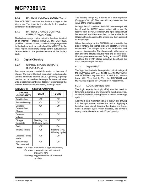
鈥?/div>
2.7V
) 脳
575mA
=
1.61W
6.2
PCB Layout Issues
With the battery charger mounted on a 1 in
2
pad of
1 oz. copper, the junction temperature rise is 60掳C,
approximately. This would allow for a maximum operat-
ing ambient temperature of 50掳C before thermal
regulation is entered.
For optimum voltage regulation, place the battery pack
as close as possible to the device鈥檚 V
BAT
and V
SS
pins.
It is recommended to minimize voltage drops along the
high current carrying PCB traces.
If the PCB layout is used as a heatsink, adding many
vias in the heatsink pad can help conduct more heat to
the back-plane of the PCB, thus reducing the maximum
junction temperature.
6.1.1.3
External Capacitors
The MCP7386X is stable with or without a battery load.
In order to maintain good AC stability in the Constant
Voltage mode, a minimum capacitance of 4.7 碌F is
recommended to bypass the V
BAT
pin to V
SS
. This
capacitance provides compensation when there is no
battery load. In addition, the battery and interconnec-
tions appear inductive at high frequencies. These
elements are in the control feedback loop during
constant voltage mode. Therefore, the bypass capaci-
tance may be necessary to compensate for the
inductive nature of the battery pack.
Virtually any good quality output filter capacitor can be
used, independent of the capacitor鈥檚 minimum Effec-
tive Series Resistance (ESR) value. The actual value of
the capacitor and its associated ESR depends on the
output load current. A 4.7 碌F ceramic, tantalum or alu-
minum electrolytic capacitor at the output is usually
sufficient to ensure stability for up to a 1A output
current.
6.1.1.4
Reverse-Blocking Protection
The MCP7386X provides protection from a faulted or
shorted input, or from a reversed-polarity input source.
Without the protection, a faulted or shorted input would
discharge the battery pack through the body diode of
the internal pass transistor.
6.1.1.5
Enable Interface
In the stand-alone configuration, the enable pin is gen-
erally tied to the input voltage. The MCP7386X auto-
matically enters a low-power mode when voltage on
the V
DD
input falls below the undervoltage lockout
voltage (V
STOP
) reducing the battery drain current to
0.23 碌A, typically.
6.1.1.6
Charge Status Interface
Two status outputs provide information on the state of
charge. The current-limited, open-drain outputs can be
used to illuminate external LEDs. Refer to Table 5-1 for
a summary of the state of the status outputs during a
charge cycle.
铮?/div>
2004 Microchip Technology Inc.
DS21893A-page 19


 1
1
 2
2
 3
3
 4
4
 5
5
 6
6
 7
7
 8
8
 9
9
 10
10
 11
11
 12
12
 13
13
 14
14
 15
15
 16
16
 17
17
 18
18
 19
19
 20
20
 21
21
 22
22
 23
23
 24
24
 25
25
 26
26
