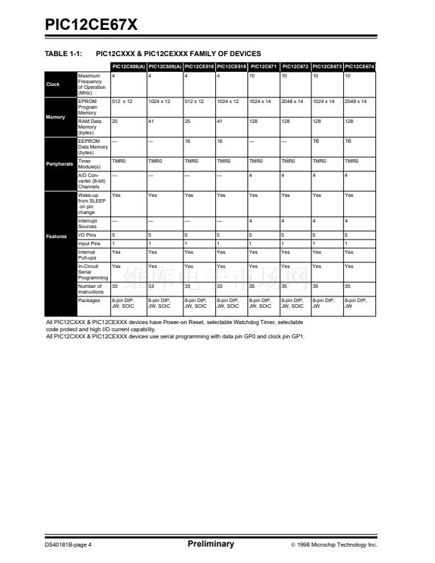
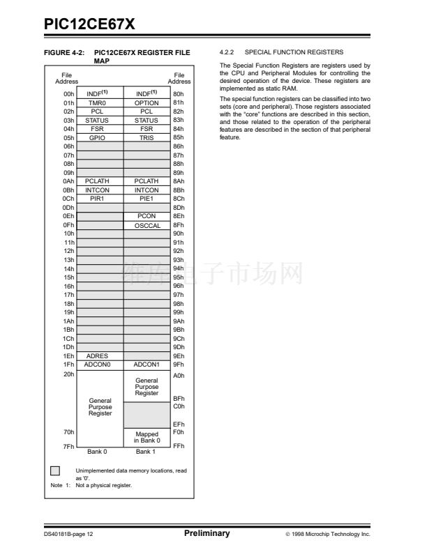
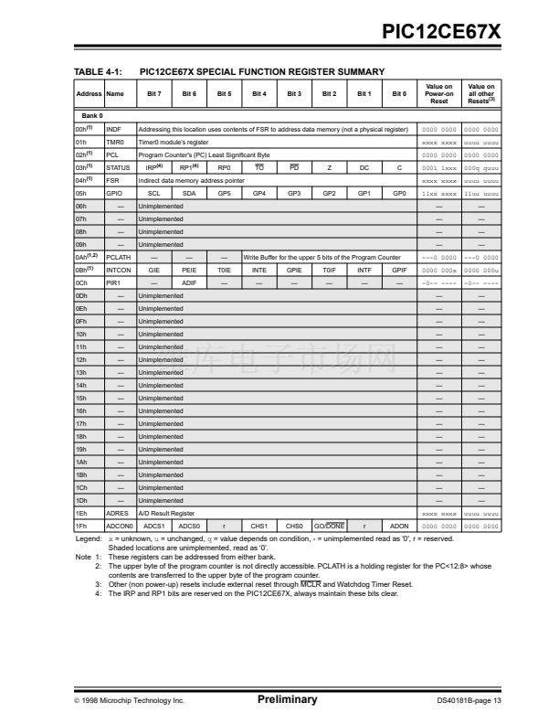
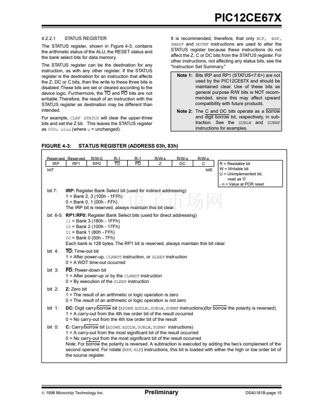
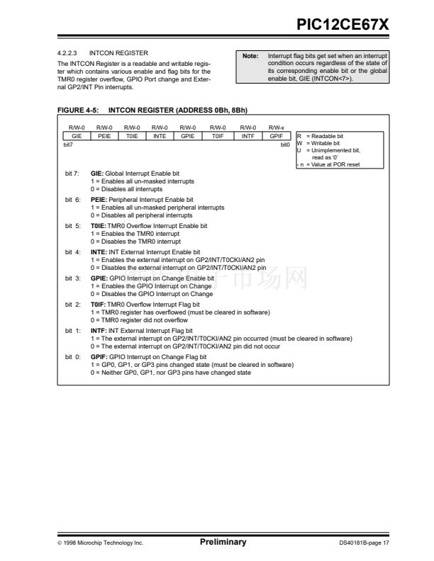
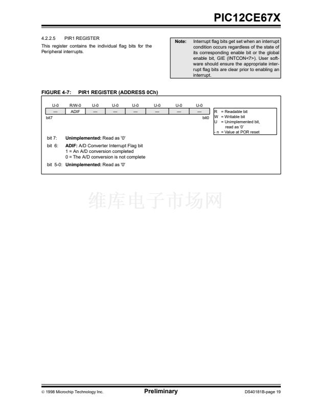
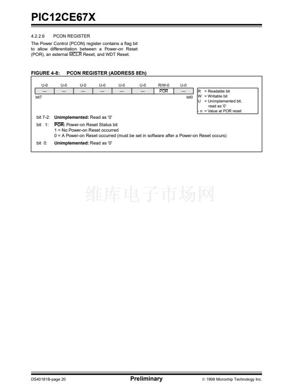
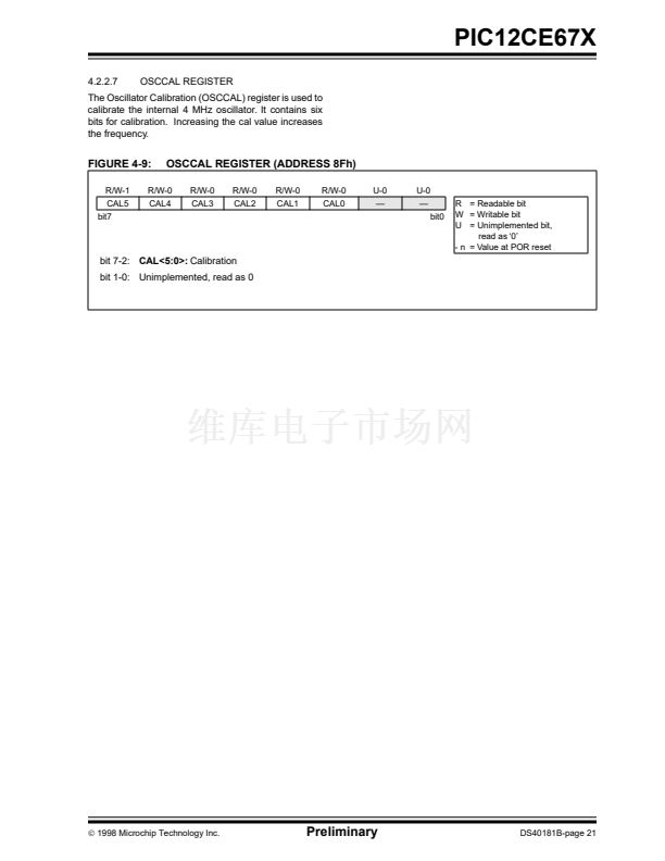
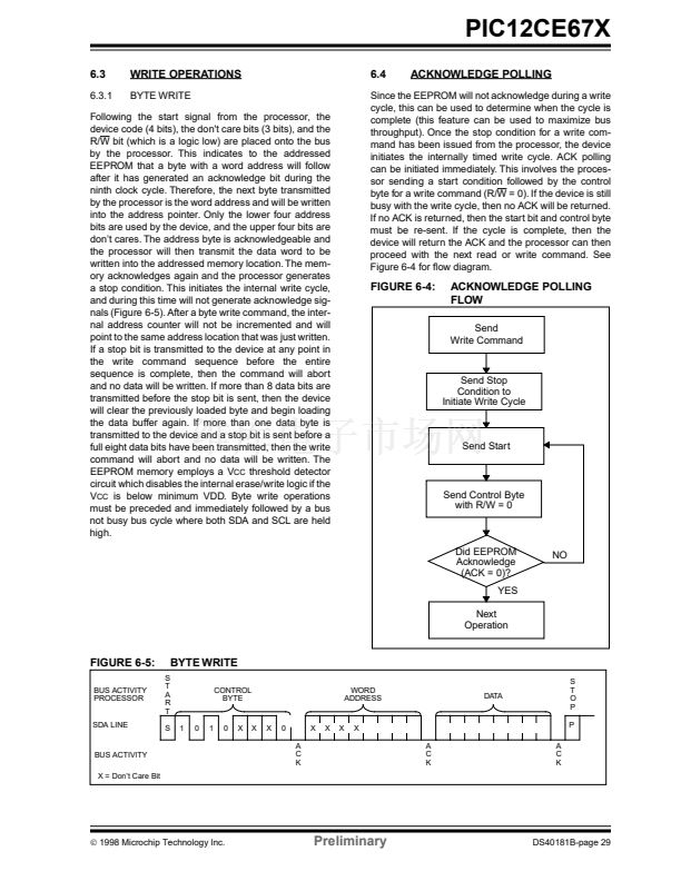
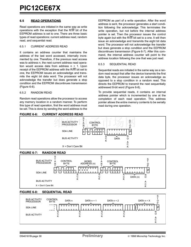
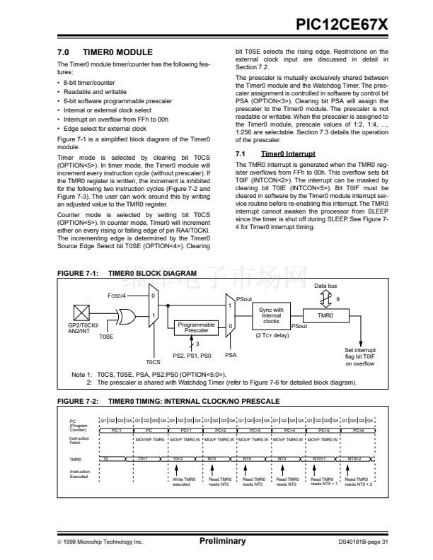
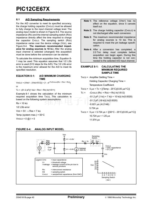
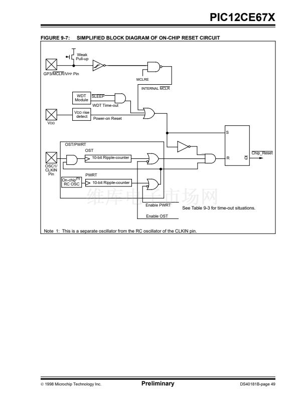
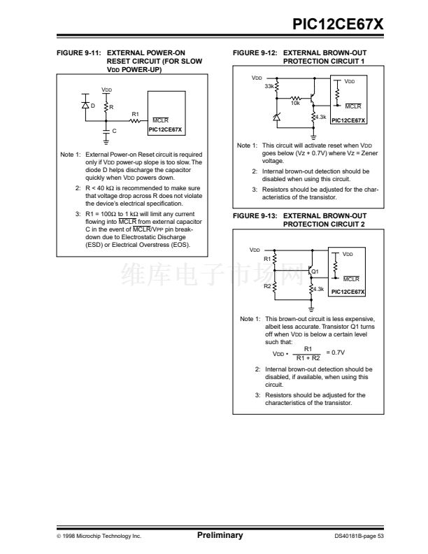
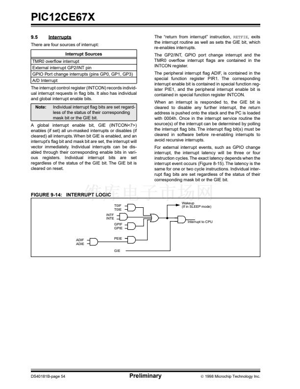
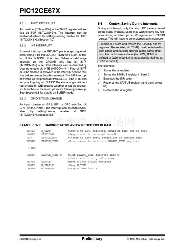
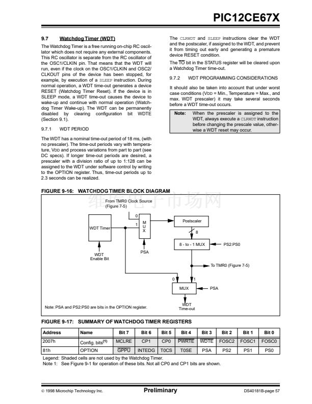
鈥?/div>
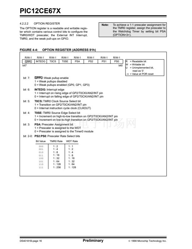
INTEDG
RP1
(1)
SDA
Bit 5
Bit 4
Bit 3
Bit 2
Bit 1
Bit 0
GPIO Data Direction Register
T0CS
RP0
GP5
T0SE
TO
GP4
PSA
PD
GP3
PS2
Z
GP2
Legend: Shaded cells not used by Port Registers, read as 鈥?鈥? 鈥?= unimplemented, read as '0',
x
= unknown,
u
= unchanged,
q = see tables in Section 9.4 for possible values.
Note 1: The IRP and RP1 bits are reserved on the PIC12CE67X, always maintain these bits clear.
5.4
5.4.1
I/O Programming Considerations
BI-DIRECTIONAL I/O PORTS
Example 5-1 shows the effect of two sequential read-
modify-write instructions on an I/O port.
Any instruction which writes, operates internally as a
read followed by a write operation. The
BCF
and
BSF
instructions, for example, read the register into the
CPU, execute the bit operation and write the result back
to the register. Caution must be used when these
instructions are applied to a port with both inputs and
outputs de铿乶ed. For example, a
BSF
operation on bit5
of GPIO will cause all eight bits of GPIO to be read into
the CPU. Then the
BSF
operation takes place on bit5
and GPIO is written to the output latches. If another bit
of GPIO is used as a bi-directional I/O pin (e.g., bit0)
and it is de铿乶ed as an input at this time, the input signal
present on the pin itself would be read into the CPU
and rewritten to the data latch of this particular pin,
overwriting the previous content. As long as the pin
stays in the input mode, no problem occurs. However,
if bit0 is switched to an output, the content of the data
latch may now be unknown.
Reading the port register, reads the values of the port
pins. Writing to the port register writes the value to the
port latch. When using read-modify-write instructions
(ex.
BCF, BSF,
etc.) on a port, the value of the port pins
is read, the desired operation is done to this value, and
this value is then written to the port latch.
EXAMPLE 5-1:
READ-MODIFY-WRITE
INSTRUCTIONS ON AN
I/O PORT
;Initial GPIO Settings
; GPIO<5:3> Inputs
; GPIO<2:0> Outputs
;
;
GPIO latch GPIO pins
;
---------- ----------
BCF
GPIO, 5
;--01 -ppp
--11 pppp
BCF
GPIO, 4
;--10 -ppp
--11 pppp
MOVLW 007h
;
TRIS GPIO
;--10 -ppp
--11 pppp
;
;Note that the user may have expected the pin
;values to be --00 pppp. The 2nd BCF caused
;GP5 to be latched as the pin value (High).
A pin actively outputting a Low or High should not be
driven from external devices at the same time in order
to change the level on this pin (鈥渨ired-or鈥? 鈥渨ired-and鈥?.
The resulting high output currents may damage the
chip.
FIGURE 5-2:
SUCCESSIVE I/O OPERATION
Q1 Q2 Q3 Q4 Q1 Q2 Q3 Q4 Q1 Q2 Q3 Q4 Q1 Q2 Q3 Q4
PC
Instruction
fetched
GP5:GP0
Port pin
written here
Instruction
executed
MOVWF GPIO
(Write to
GPIO)
Port pin
sampled here
MOVF GPIO,W
(Read
GPIO)
NOP
MOVWF GPIO
PC + 1
MOVF GPIO,W
PC + 2
NOP
PC + 3
NOP
This example shows a write to GPIO followed
by a read from GPIO.
Data setup time = (0.25 T
CY
鈥?T
PD
)
where: T
CY
= instruction cycle.
T
PD
= propagation delay
Therefore, at higher clock frequencies, a
write followed by a read may be problematic.
DS40181B-page 26
Preliminary
漏
1998 Microchip Technology Inc.


 1
1
 2
2
 3
3
 4
4
 5
5
 6
6
 7
7
 8
8
 9
9
 10
10
 11
11
 12
12
 13
13
 14
14
 15
15
 16
16
 17
17
 18
18
 19
19
 20
20
 21
21
 22
22
 23
23
 24
24
 25
25
 26
26
 27
27
 28
28
 29
29
 30
30
 31
31
 32
32
 33
33
 34
34
 35
35
 36
36
 37
37
 38
38
 39
39
 40
40
 41
41
 42
42
 43
43
 44
44
 45
45
 46
46
 47
47
 48
48
 49
49
 50
50
 51
51
 52
52
 53
53
 54
54
 55
55
 56
56
 57
57
 58
58
 59
59
 60
60
 61
61
 62
62
 63
63
 64
64
 65
65
 66
66
 67
67
 68
68
 69
69
 70
70
 71
71
 72
72
 73
73
 74
74
 75
75
 76
76
 77
77
 78
78
 79
79
 80
80
 81
81
 82
82
 83
83
 84
84
 85
85
 86
86
 87
87
 88
88
 89
89
 90
90
 91
91
 92
92
 93
93
 94
94
 95
95
 96
96
 97
97
 98
98
 99
99
 100
100
 101
101
 102
102
 103
103
 104
104
 105
105
 106
106
 107
107
 108
108
 109
109
 110
110
 111
111
 112
112
 113
113
 114
114
 115
115
 116
116
