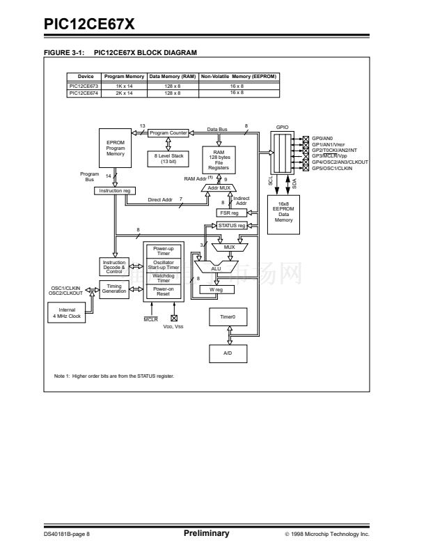
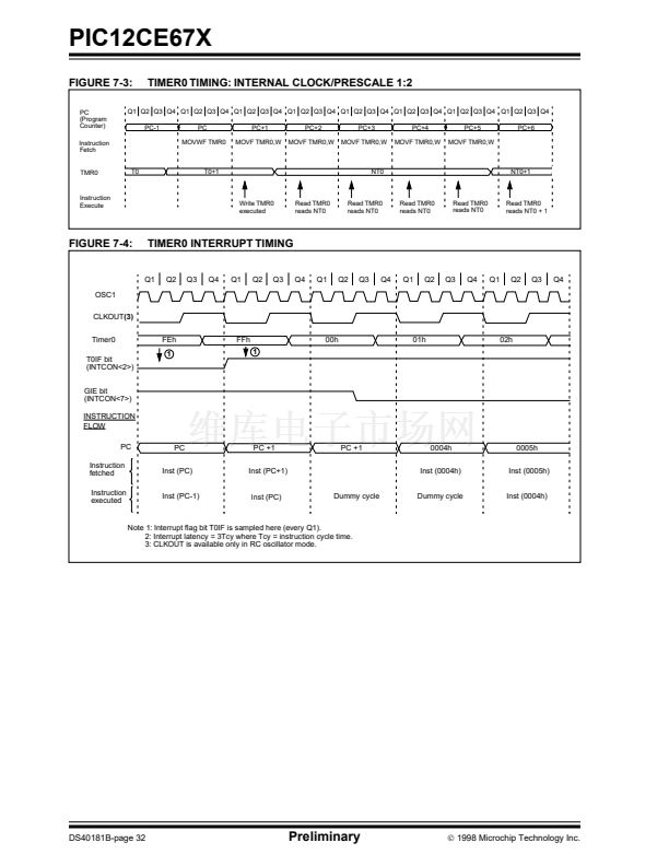
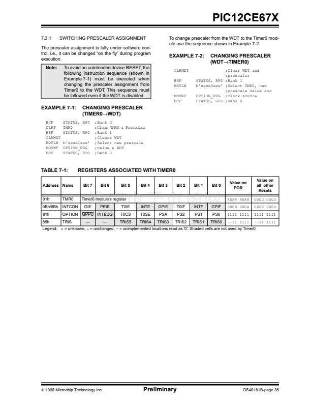
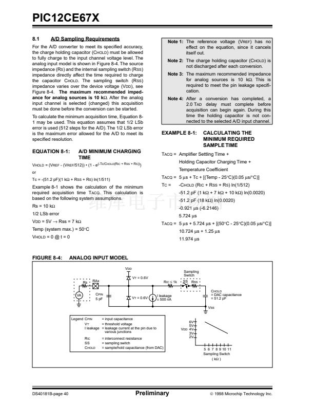
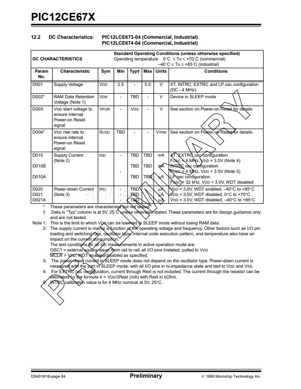
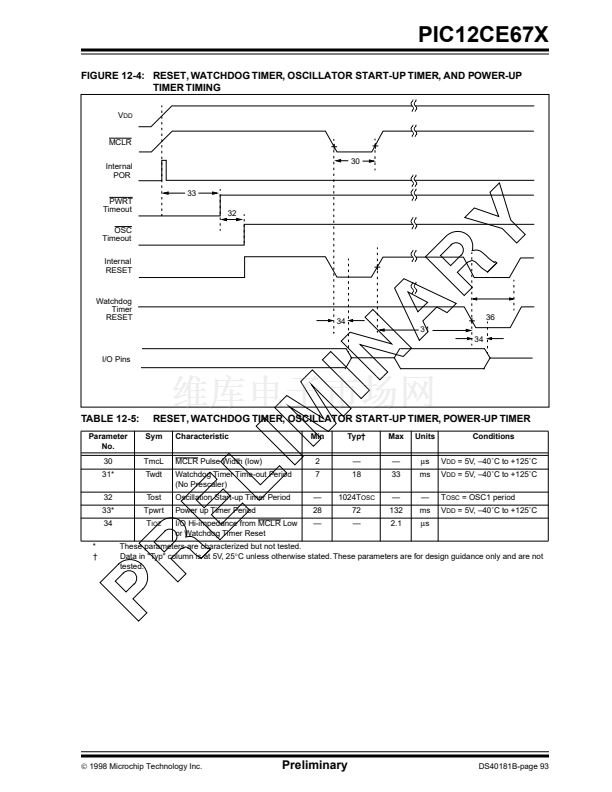
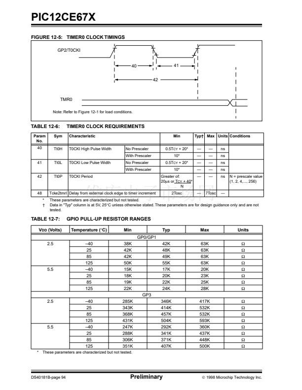
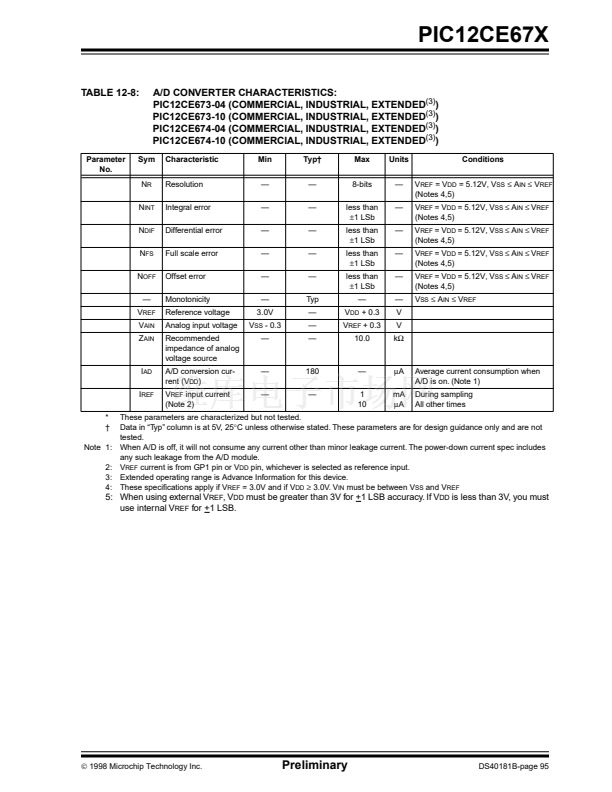
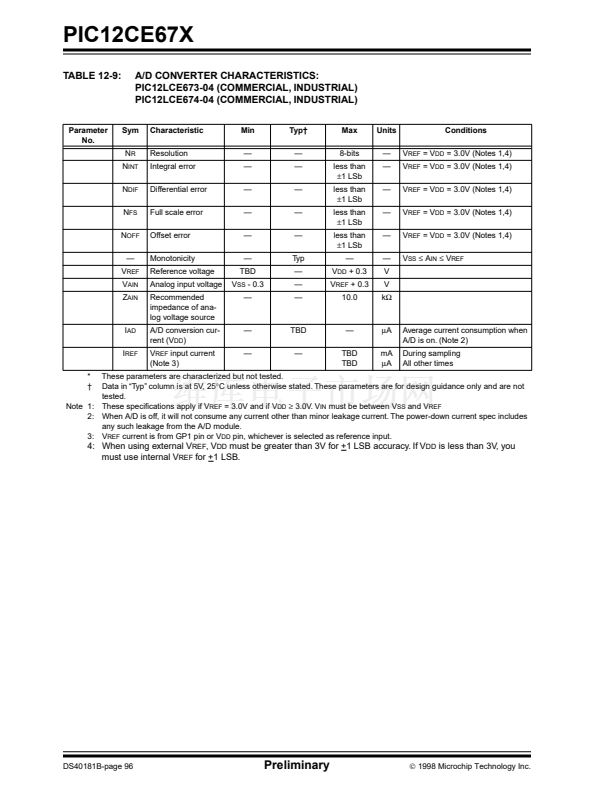
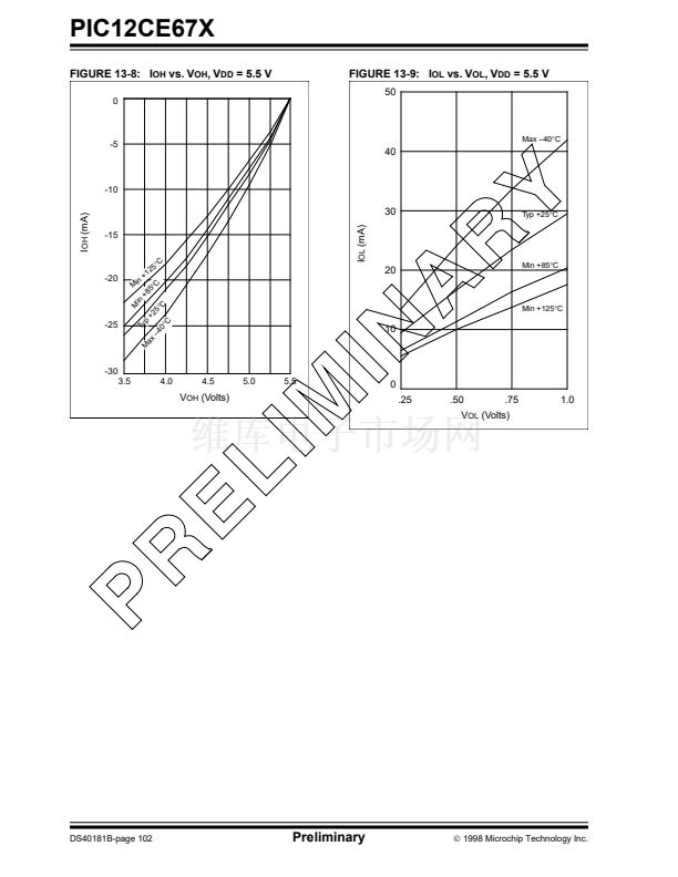
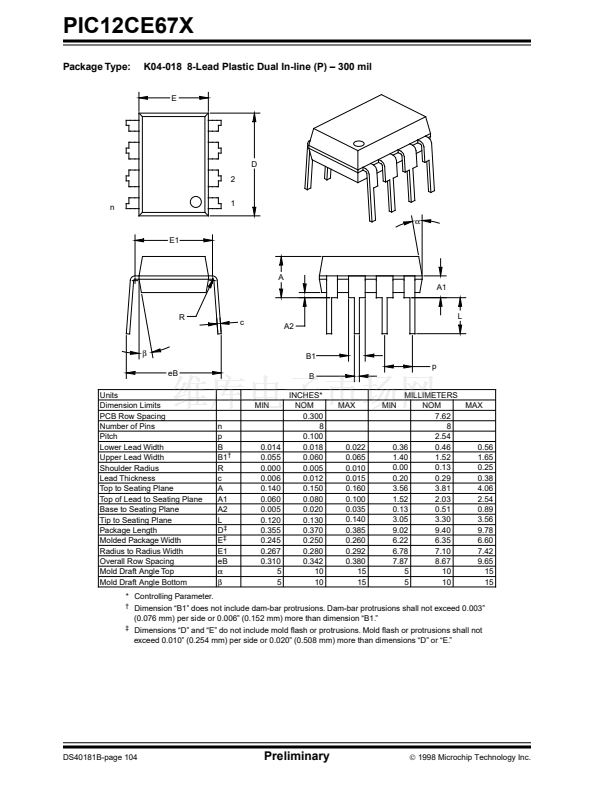
PIC12CE67X
6.0
EEPROM PERIPHERAL
OPERATION
鈥?Data transfer may be initiated only when the bus
is not busy.
During data transfer, the data line must remain stable
whenever the clock line is HIGH. Changes in the data
line while the clock line is HIGH will be interpreted as a
START or STOP condition.
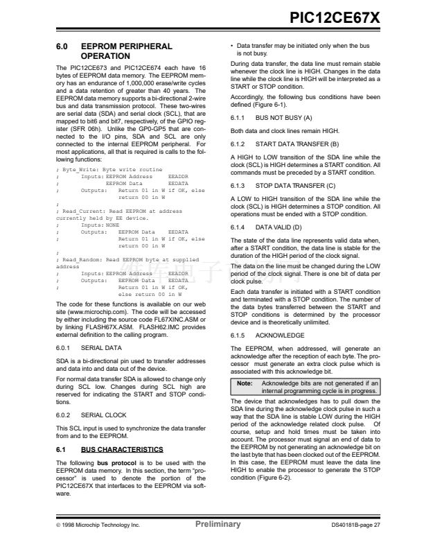
Accordingly, the following bus conditions have been
de铿乶ed (Figure 6-1).
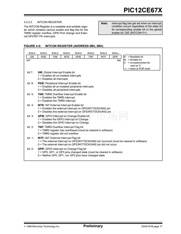
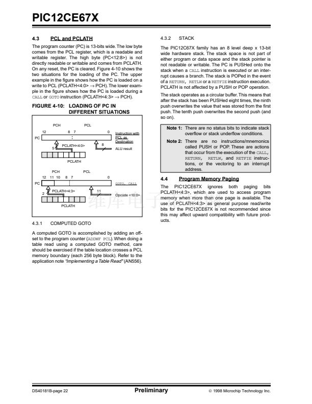
6.1.1
BUS NOT BUSY (A)
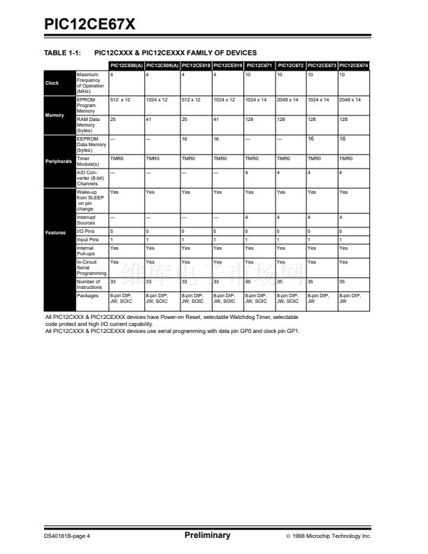
The PIC12CE673 and PIC12CE674 each have 16
bytes of EEPROM data memory. The EEPROM mem-
ory has an endurance of 1,000,000 erase/write cycles
and a data retention of greater than 40 years. The
EEPROM data memory supports a bi-directional 2-wire
bus and data transmission protocol. These two-wires
are serial data (SDA) and serial clock (SCL), that are
mapped to bit6 and bit7, respectively, of the GPIO reg-
ister (SFR 06h). Unlike the GP0-GP5 that are con-
nected to the I/O pins, SDA and SCL are only
connected to the internal EEPROM peripheral. For
most applications, all that is required is calls to the fol-
lowing functions:
; Byte_Write: Byte write routine
;
Inputs: EEPROM Address
EEADDR
;
EEPROM Data
EEDATA
;
Outputs:
Return 01 in W if OK, else
return 00 in W
;
; Read_Current: Read EEPROM at address
currently held by EE device.
;
Inputs: NONE
;
Outputs:
EEPROM Data
EEDATA
;
Return 01 in W if OK, else
return 00 in W
;
; Read_Random: Read EEPROM byte at supplied
address
;
Inputs: EEPROM Address
EEADDR
;
Outputs:
EEPROM Data
EEDATA
;
Return 01 in W if OK,
else return 00 in W
Both data and clock lines remain HIGH.
6.1.2
START DATA TRANSFER (B)
A HIGH to LOW transition of the SDA line while the
clock (SCL) is HIGH determines a START condition. All
commands must be preceded by a START condition.
6.1.3
STOP DATA TRANSFER (C)
A LOW to HIGH transition of the SDA line while the
clock (SCL) is HIGH determines a STOP condition. All
operations must be ended with a STOP condition.
6.1.4
DATA VALID (D)
The state of the data line represents valid data when,
after a START condition, the data line is stable for the
duration of the HIGH period of the clock signal.
The data on the line must be changed during the LOW
period of the clock signal. There is one bit of data per
clock pulse.
Each data transfer is initiated with a START condition
and terminated with a STOP condition. The number of
the data bytes transferred between the START and
STOP conditions is determined by the processor
device and is theoretically unlimited.
6.1.5
ACKNOWLEDGE
The code for these functions is available on our web
site (www.microchip.com). The code will be accessed
by either including the source code FL67XINC.ASM or
by linking FLASH67X.ASM. FLASH62.IMC provides
external de铿乶ition to the calling program.
6.0.1
SERIAL DATA
SDA is a bi-directional pin used to transfer addresses
and data into and data out of the device.
For normal data transfer SDA is allowed to change only
during SCL low. Changes during SCL high are
reserved for indicating the START and STOP condi-
tions.
6.0.2
SERIAL CLOCK
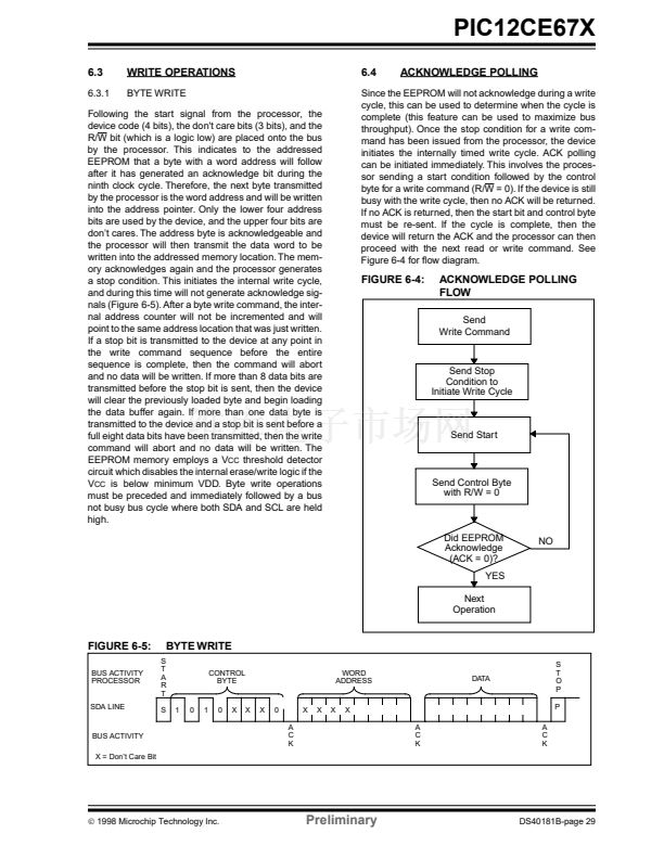
The EEPROM, when addressed, will generate an
acknowledge after the reception of each byte. The pro-
cessor must generate an extra clock pulse which is
associated with this acknowledge bit.
Note:
Acknowledge bits are not generated if an
internal programming cycle is in progress.
This SCL input is used to synchronize the data transfer
from and to the EEPROM.
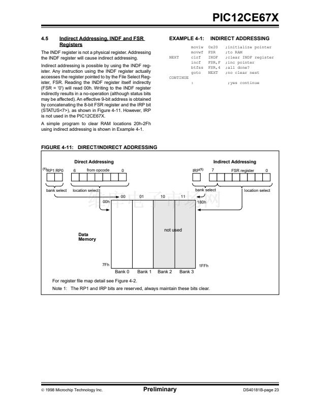
6.1
BUS CHARACTERISTICS
The following
bus protocol
is to be used with the
EEPROM data memory. In this section, the term 鈥減ro-
cessor鈥?is used to denote the portion of the
PIC12CE67X that interfaces to the EEPROM via soft-
ware.
The device that acknowledges has to pull down the
SDA line during the acknowledge clock pulse in such a
way that the SDA line is stable LOW during the HIGH
period of the acknowledge related clock pulse. Of
course, setup and hold times must be taken into
account. The processor must signal an end of data to
the EEPROM by not generating an acknowledge bit on
the last byte that has been clocked out of the EEPROM.
In this case, the EEPROM must leave the data line
HIGH to enable the processor to generate the STOP
condition (Figure 6-2).
漏
1998 Microchip Technology Inc.
Preliminary
DS40181B-page 27


 1
1
 2
2
 3
3
 4
4
 5
5
 6
6
 7
7
 8
8
 9
9
 10
10
 11
11
 12
12
 13
13
 14
14
 15
15
 16
16
 17
17
 18
18
 19
19
 20
20
 21
21
 22
22
 23
23
 24
24
 25
25
 26
26
 27
27
 28
28
 29
29
 30
30
 31
31
 32
32
 33
33
 34
34
 35
35
 36
36
 37
37
 38
38
 39
39
 40
40
 41
41
 42
42
 43
43
 44
44
 45
45
 46
46
 47
47
 48
48
 49
49
 50
50
 51
51
 52
52
 53
53
 54
54
 55
55
 56
56
 57
57
 58
58
 59
59
 60
60
 61
61
 62
62
 63
63
 64
64
 65
65
 66
66
 67
67
 68
68
 69
69
 70
70
 71
71
 72
72
 73
73
 74
74
 75
75
 76
76
 77
77
 78
78
 79
79
 80
80
 81
81
 82
82
 83
83
 84
84
 85
85
 86
86
 87
87
 88
88
 89
89
 90
90
 91
91
 92
92
 93
93
 94
94
 95
95
 96
96
 97
97
 98
98
 99
99
 100
100
 101
101
 102
102
 103
103
 104
104
 105
105
 106
106
 107
107
 108
108
 109
109
 110
110
 111
111
 112
112
 113
113
 114
114
 115
115
 116
116
