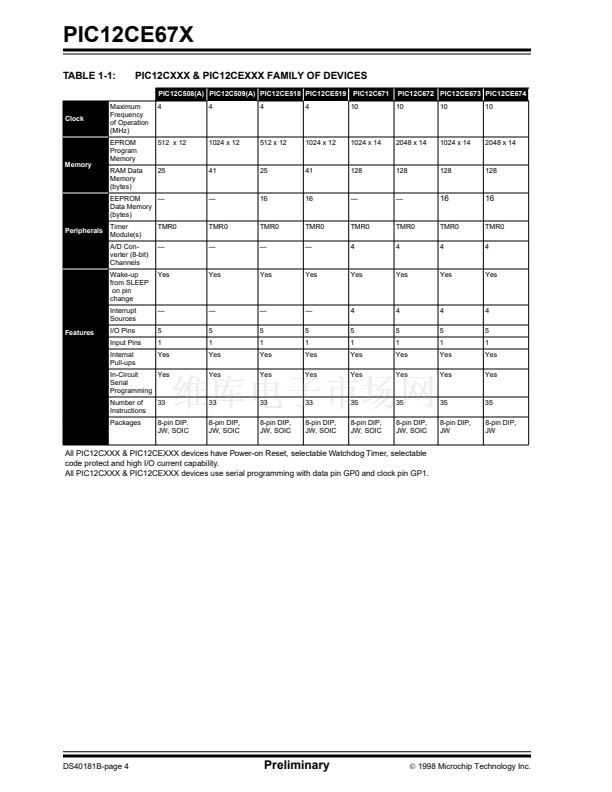
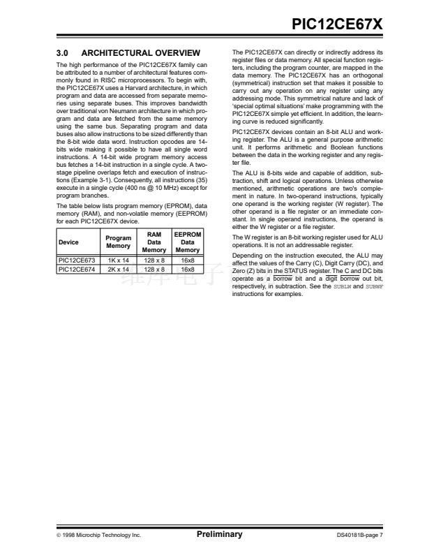
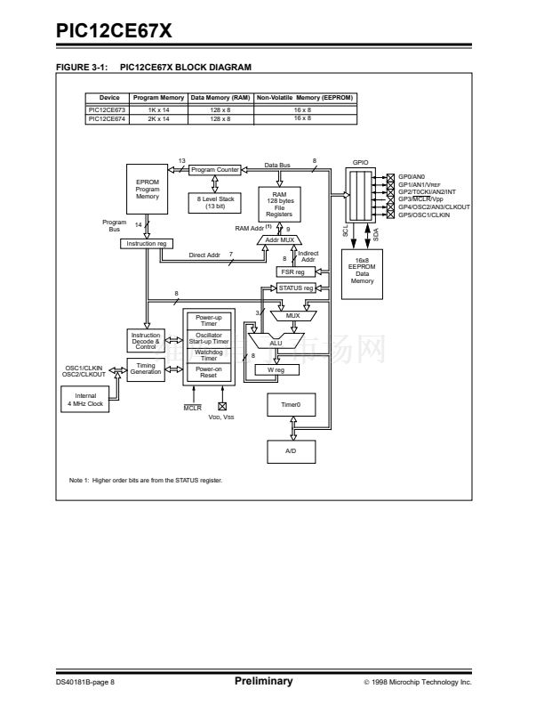
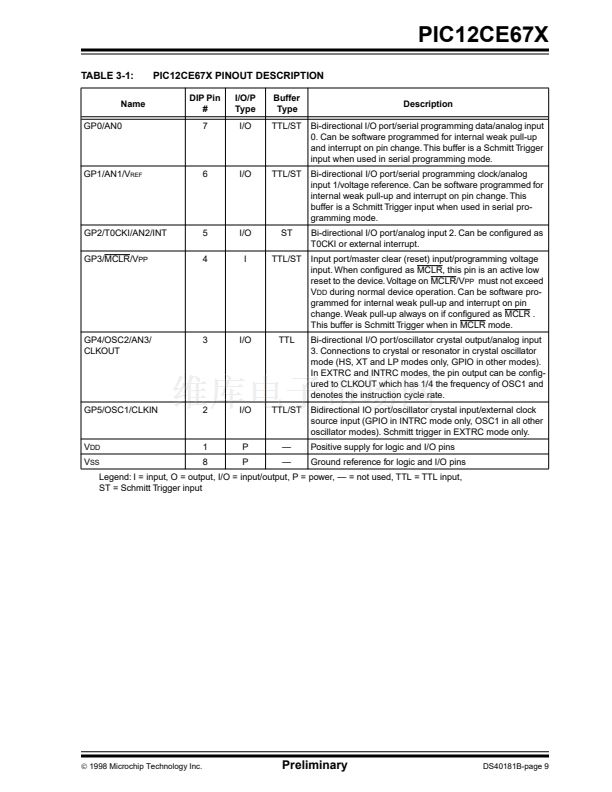
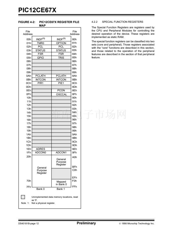
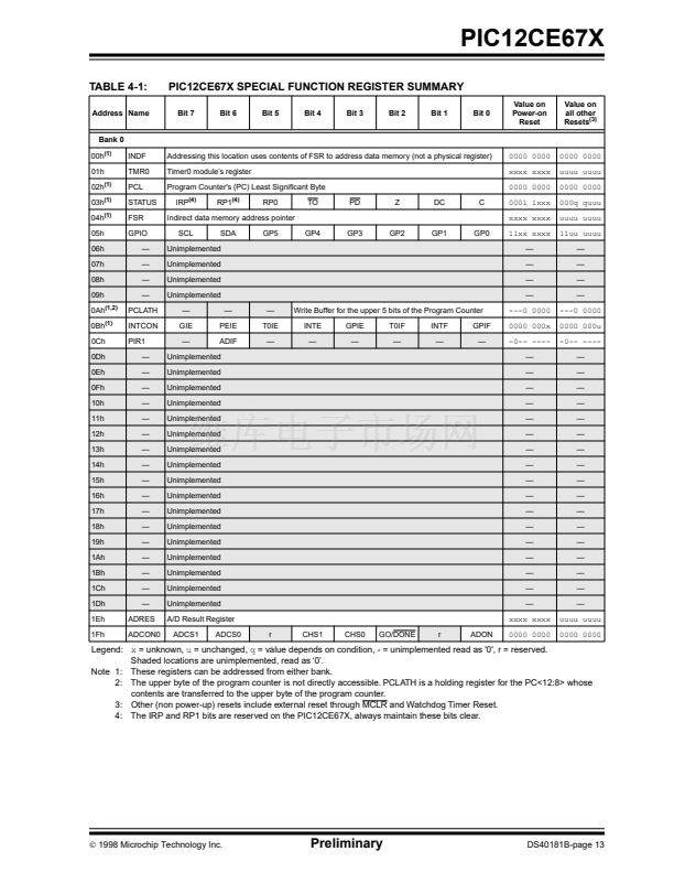
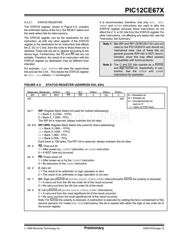
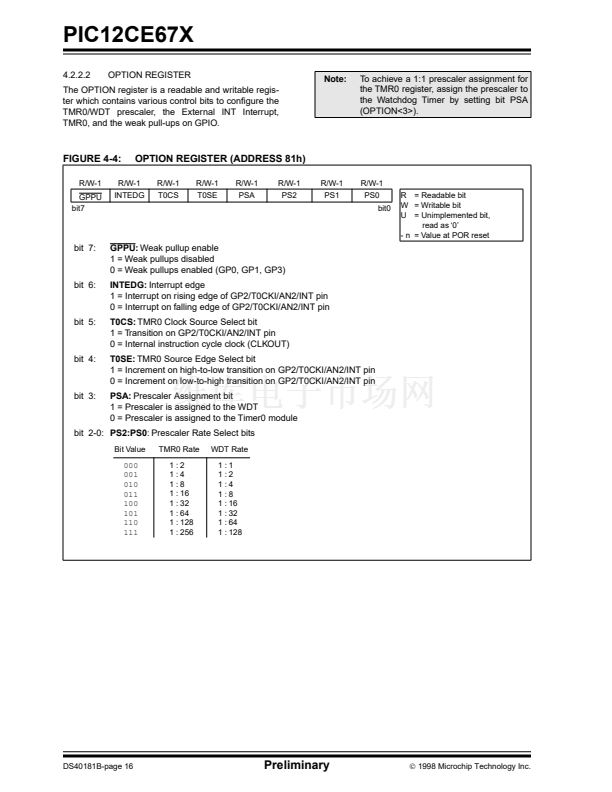
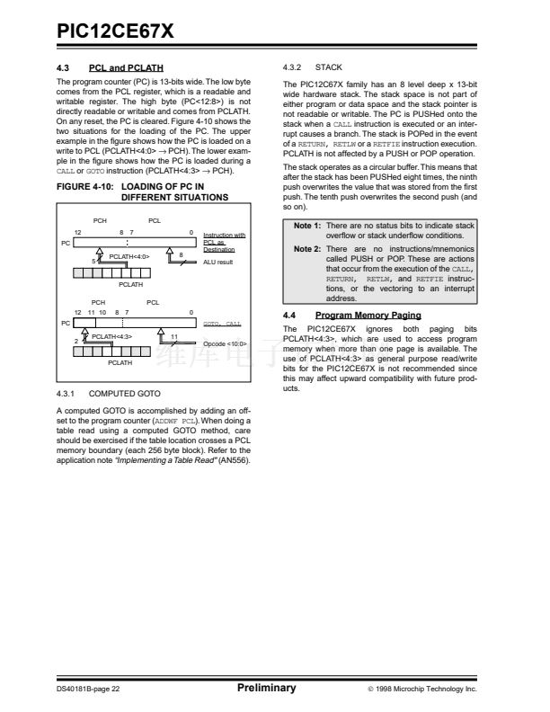
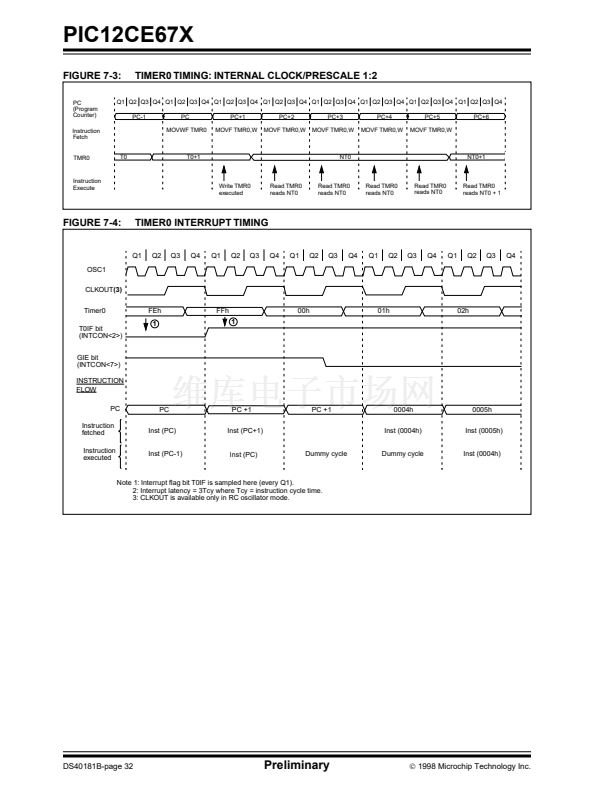
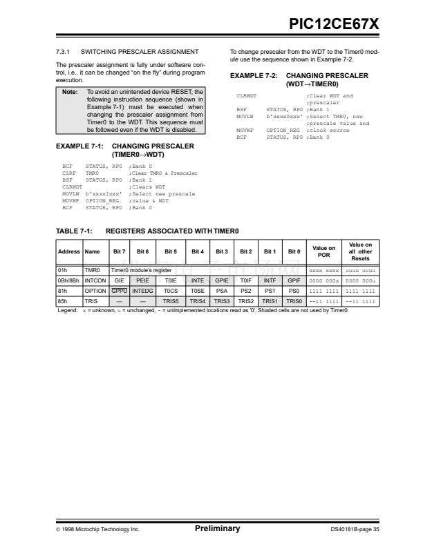
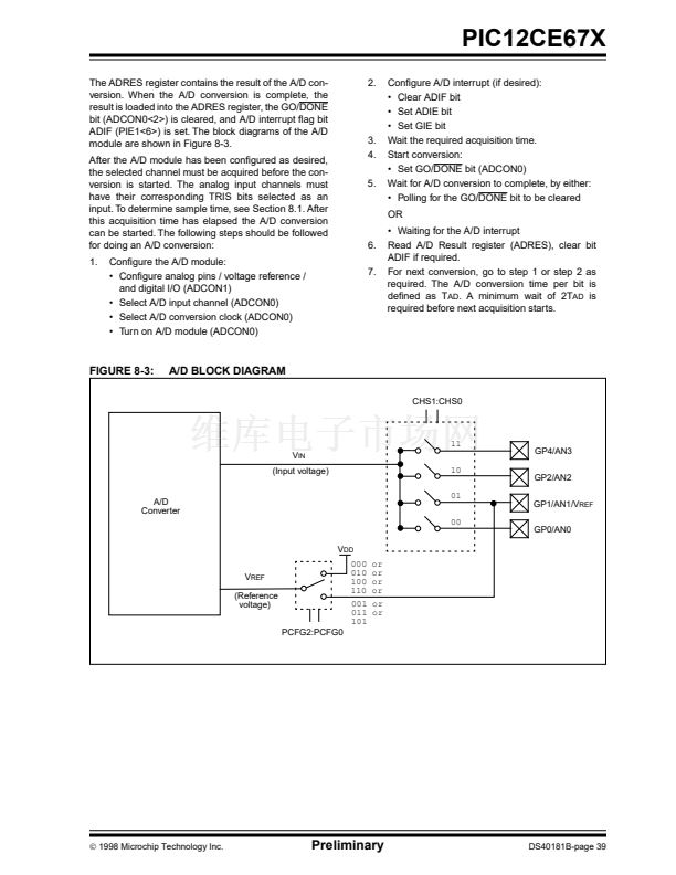
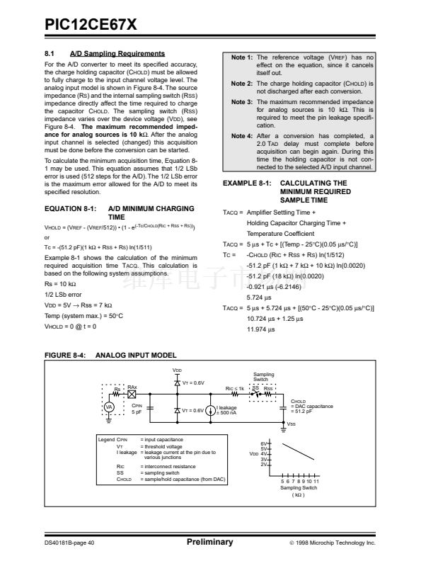
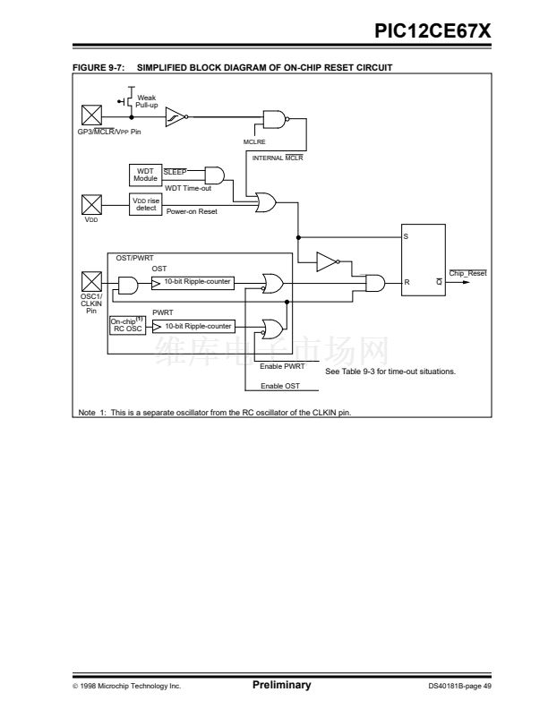
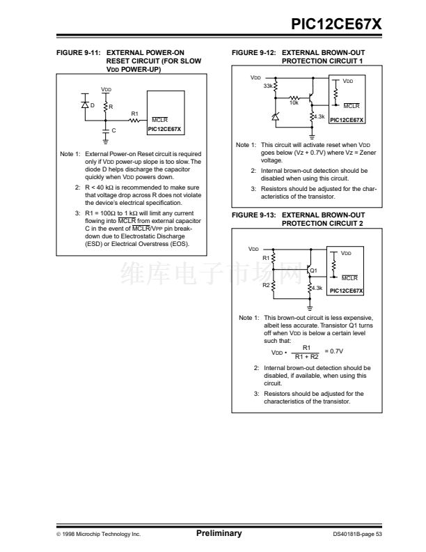
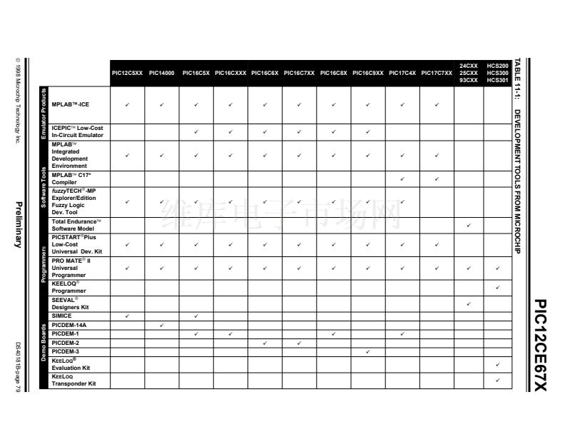
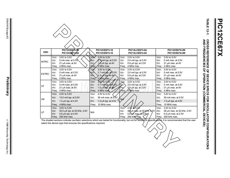
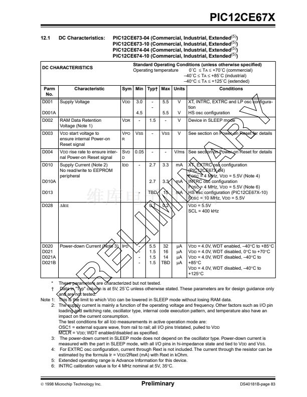
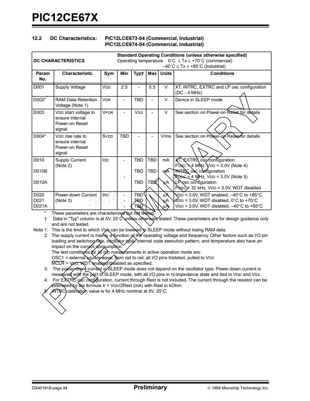
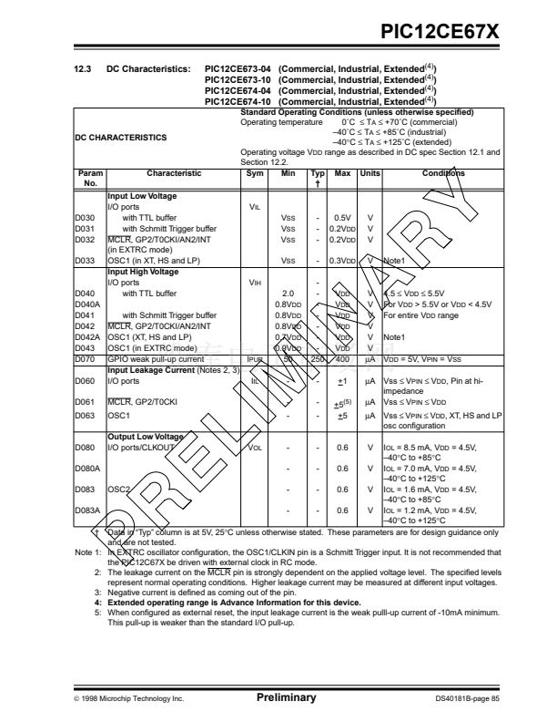
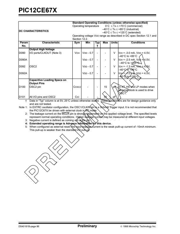
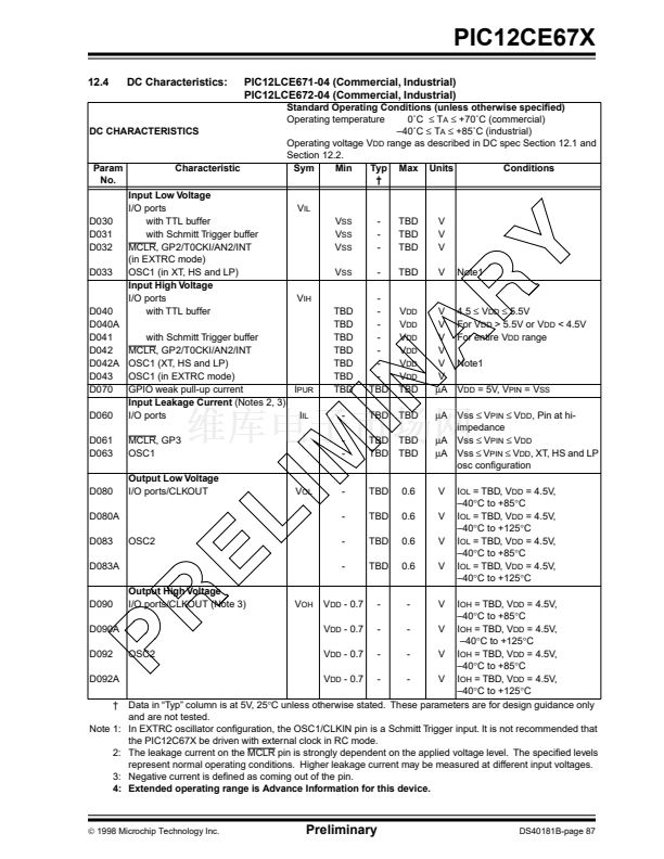
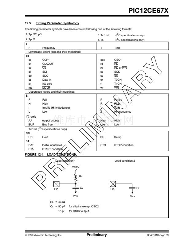
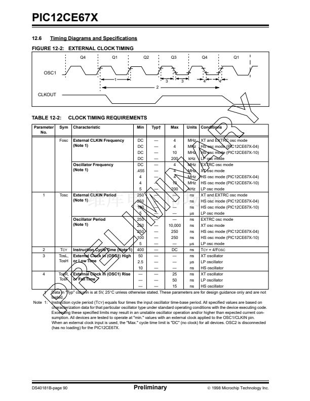
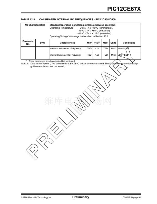
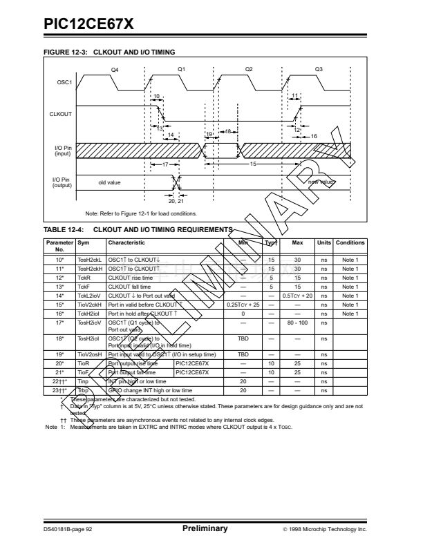
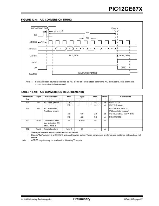
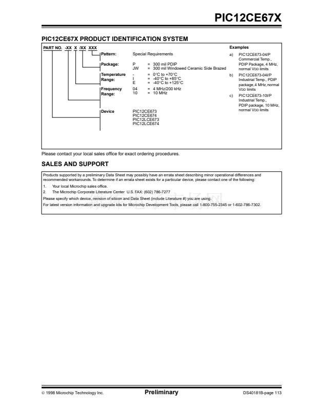
PIC12CE67X
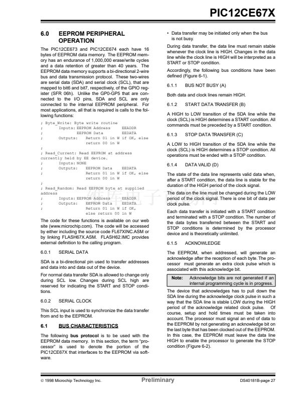
FIGURE 6-1:
SCL
(A)
(B)
DATA TRANSFER SEQUENCE ON THE SERIAL BUS
(C)
(D)
(C)
(A)
SDA
START
CONDITION
ADDRESS OR
ACKNOWLEDGE
VALID
DATA
ALLOWED
TO CHANGE
STOP
CONDITION
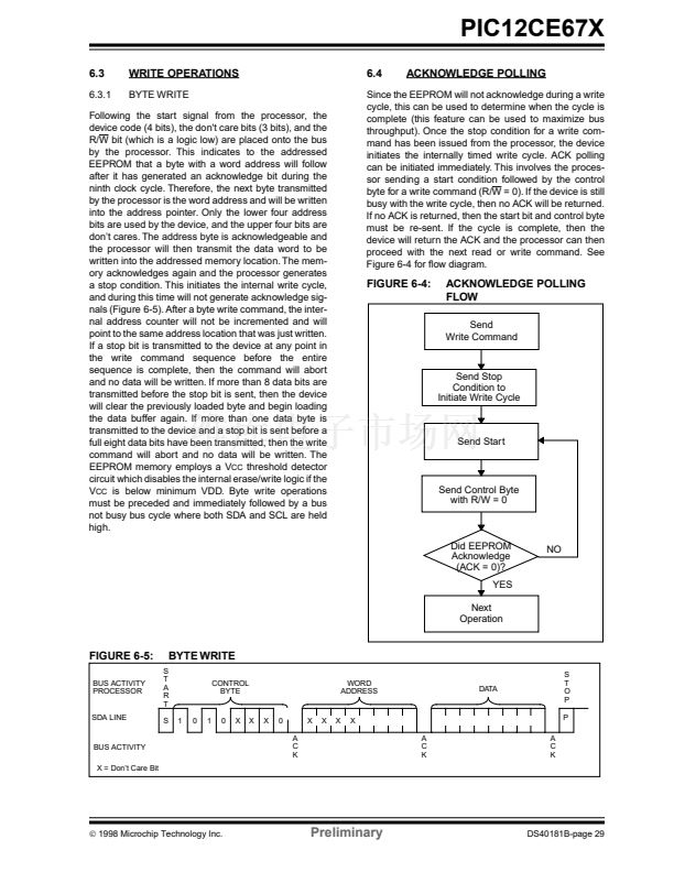
FIGURE 6-2:
ACKNOWLEDGE TIMING
Acknowledge
Bit
SCL
SDA
1
2
3
4
5
6
7
8
9
1
2
3
Data from transmitter
Transmitter must release the SDA line at this point
allowing the Receiver to pull the SDA line low to
acknowledge the previous eight bits of data.
Data from transmitter
Receiver must release the SDA line at this point
so the Transmitter can continue sending data.
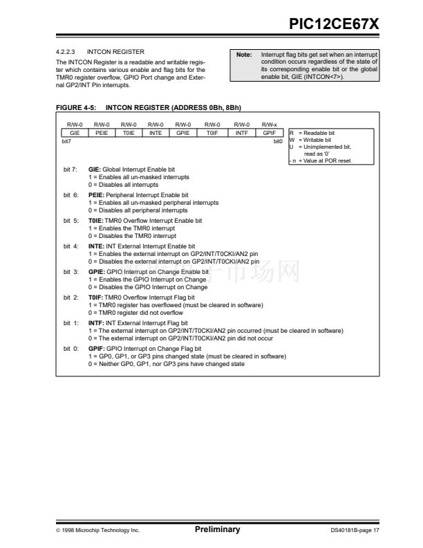
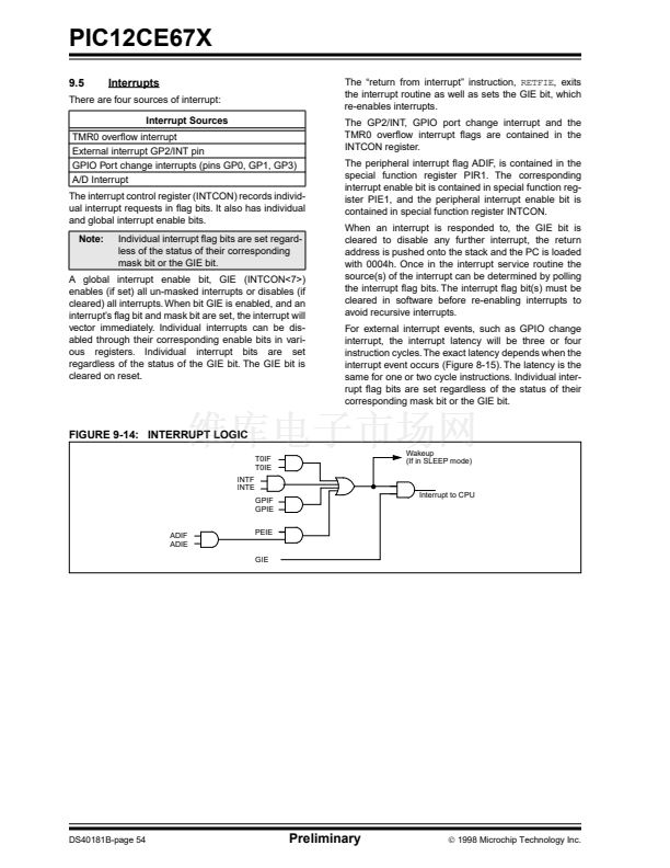
6.2
Device Addressing
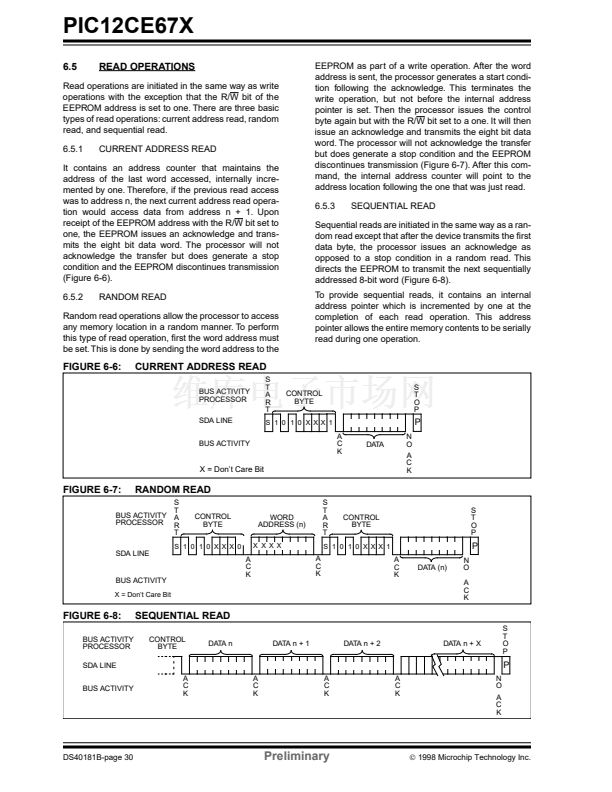
FIGURE 6-3:
CONTROL BYTE FORMAT
Read/Write Bit
After generating a START condition, the processor
transmits a control byte consisting of a EEPROM
address and a Read/Write bit that indicates what type
of operation is to be performed. The EEPROM address
consists of a 4-bit device code (1010) followed by three
don't care bits.
The last bit of the control byte determines the operation
to be performed. When set to a one a read operation is
selected, and when set to a zero a write operation is
selected. (Figure 6-3). The bus is monitored for its cor-
responding EEPROM address all the time. It generates
an acknowledge bit if the EEPROM address was true
and it is not in a programming mode.
Device Select
Bits
Don鈥檛 Care
Bits
0
X
X
X R/W ACK
S
1
0
1
EEPROM Address
Start Bit
Acknowledge Bit
DS40181B-page 28
Preliminary
漏
1998 Microchip Technology Inc.


 1
1
 2
2
 3
3
 4
4
 5
5
 6
6
 7
7
 8
8
 9
9
 10
10
 11
11
 12
12
 13
13
 14
14
 15
15
 16
16
 17
17
 18
18
 19
19
 20
20
 21
21
 22
22
 23
23
 24
24
 25
25
 26
26
 27
27
 28
28
 29
29
 30
30
 31
31
 32
32
 33
33
 34
34
 35
35
 36
36
 37
37
 38
38
 39
39
 40
40
 41
41
 42
42
 43
43
 44
44
 45
45
 46
46
 47
47
 48
48
 49
49
 50
50
 51
51
 52
52
 53
53
 54
54
 55
55
 56
56
 57
57
 58
58
 59
59
 60
60
 61
61
 62
62
 63
63
 64
64
 65
65
 66
66
 67
67
 68
68
 69
69
 70
70
 71
71
 72
72
 73
73
 74
74
 75
75
 76
76
 77
77
 78
78
 79
79
 80
80
 81
81
 82
82
 83
83
 84
84
 85
85
 86
86
 87
87
 88
88
 89
89
 90
90
 91
91
 92
92
 93
93
 94
94
 95
95
 96
96
 97
97
 98
98
 99
99
 100
100
 101
101
 102
102
 103
103
 104
104
 105
105
 106
106
 107
107
 108
108
 109
109
 110
110
 111
111
 112
112
 113
113
 114
114
 115
115
 116
116
