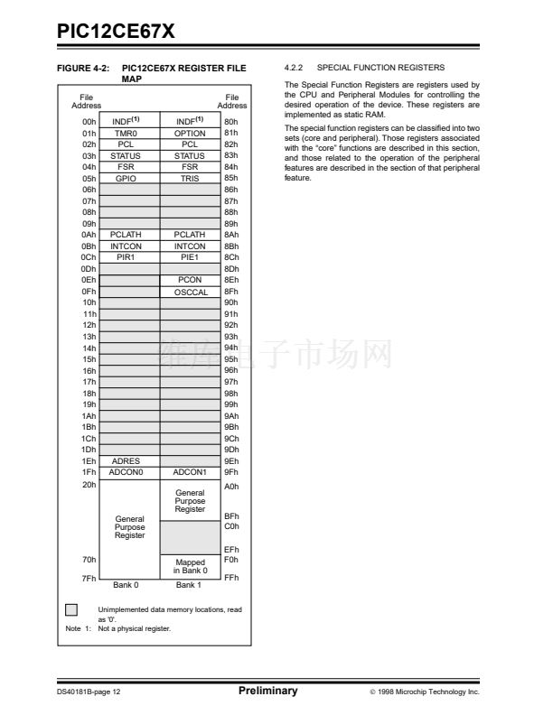
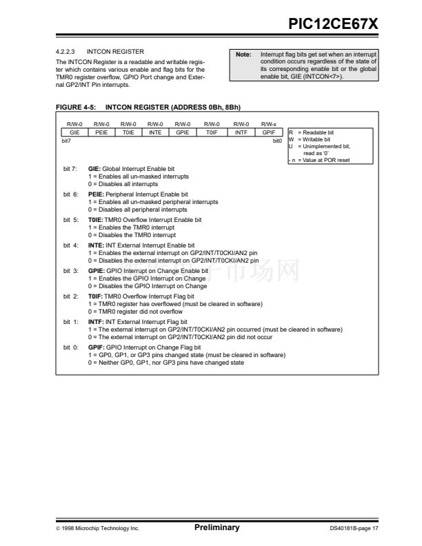
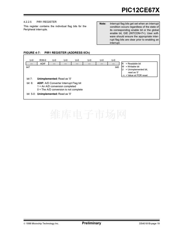
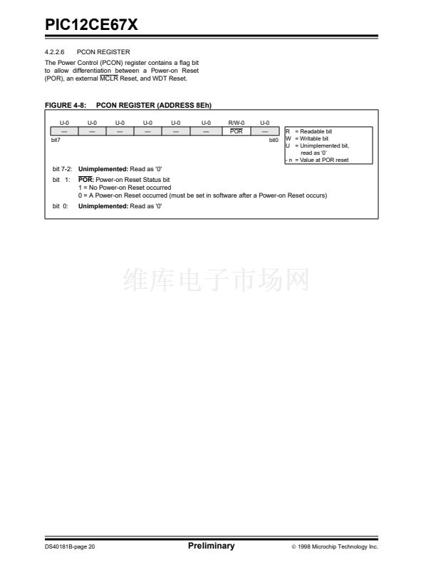
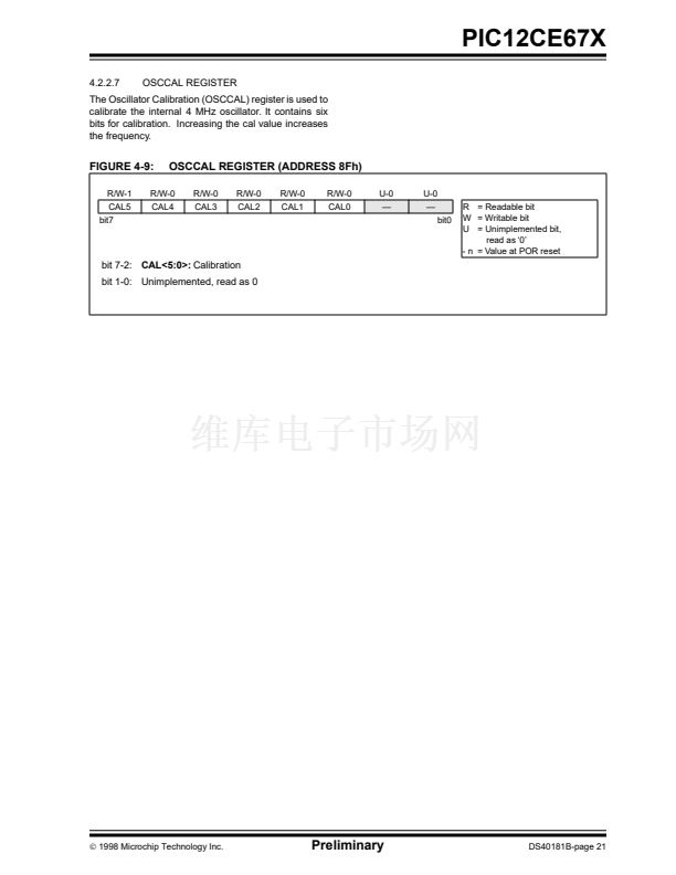
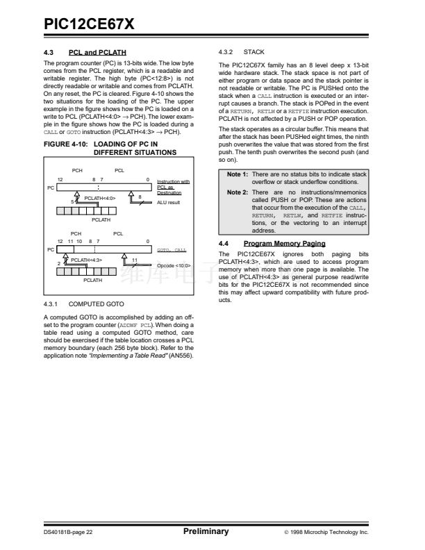
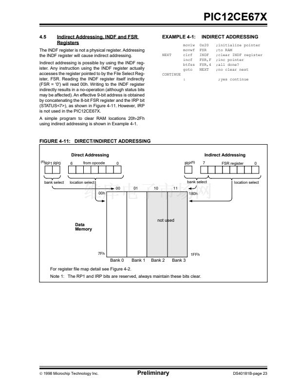
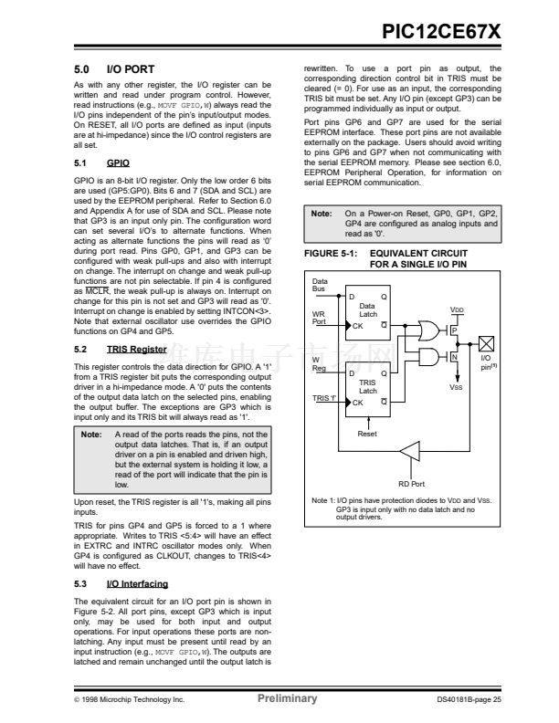
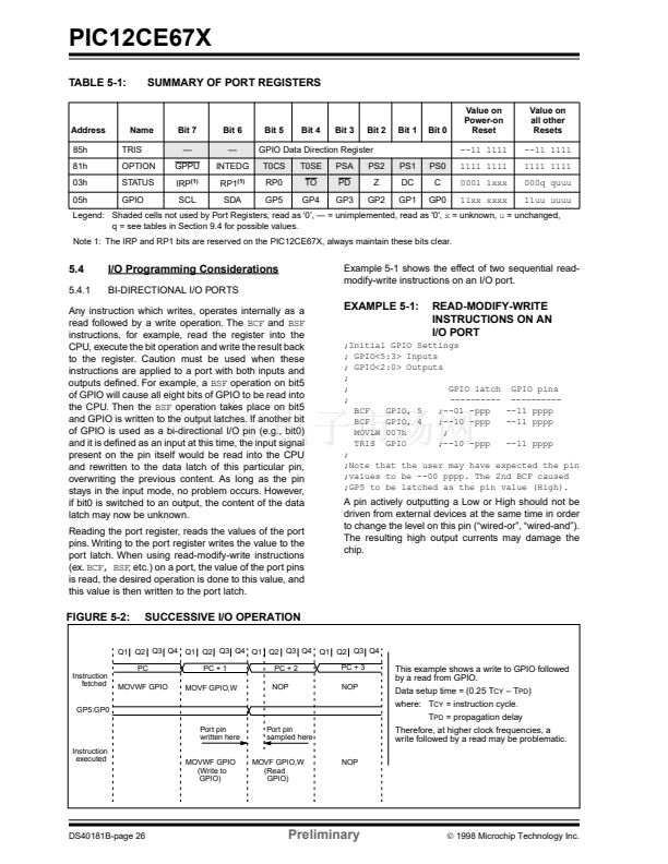
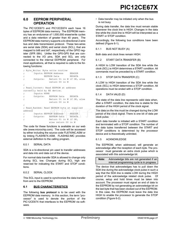
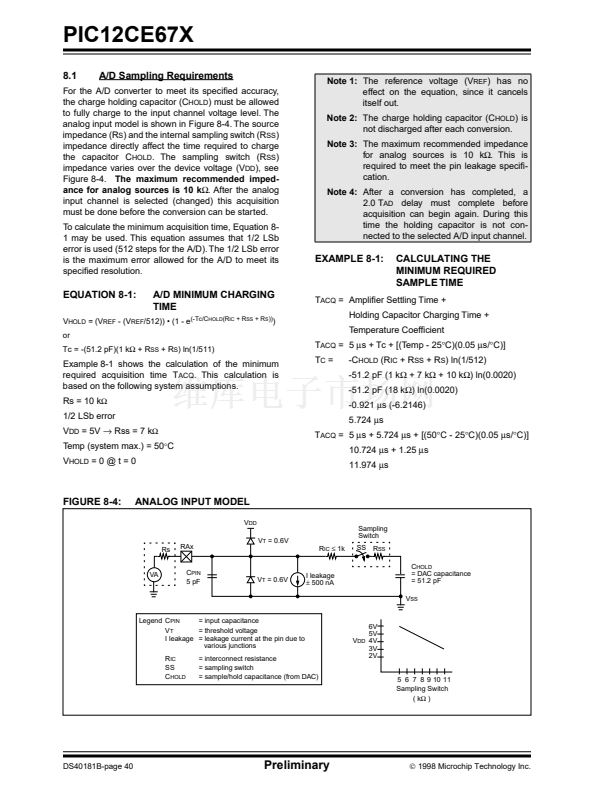
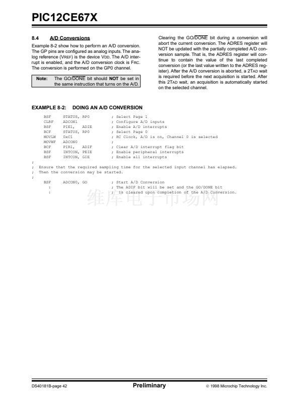
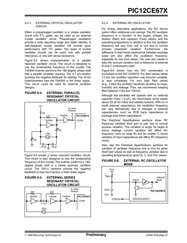
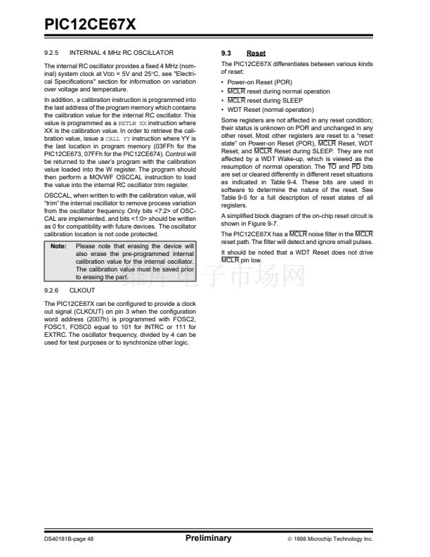
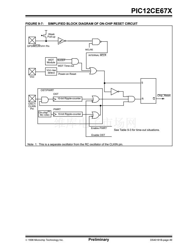
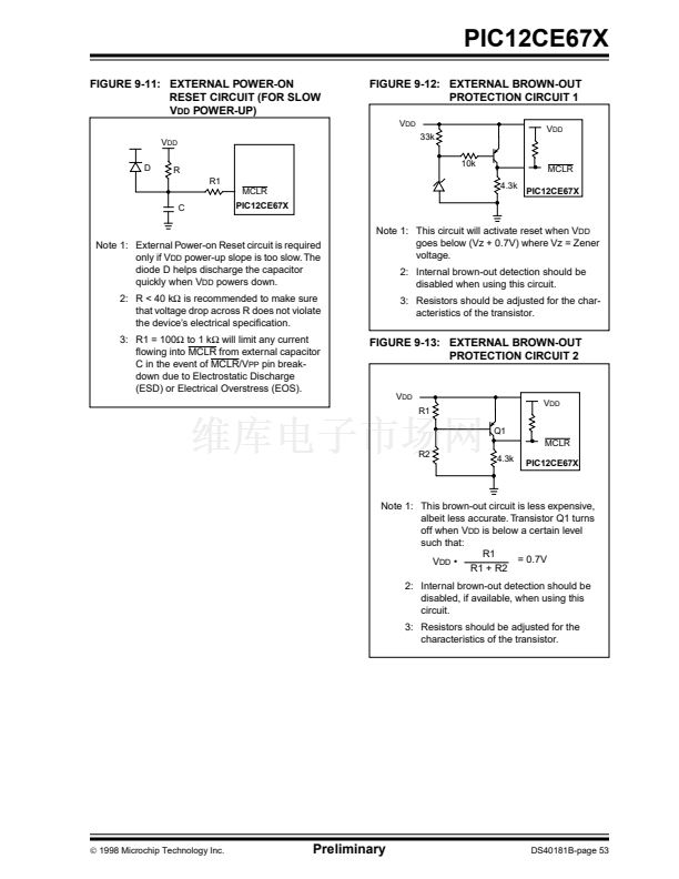
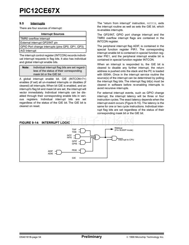
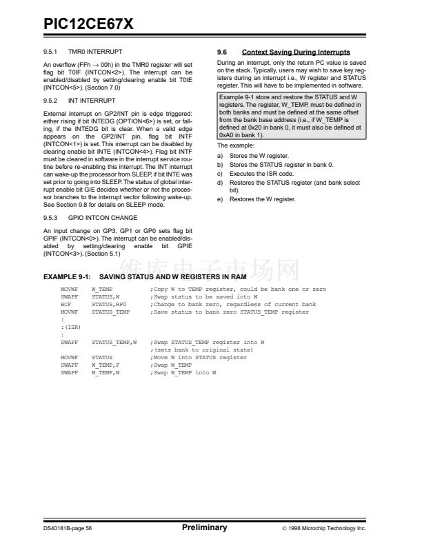
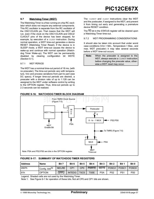
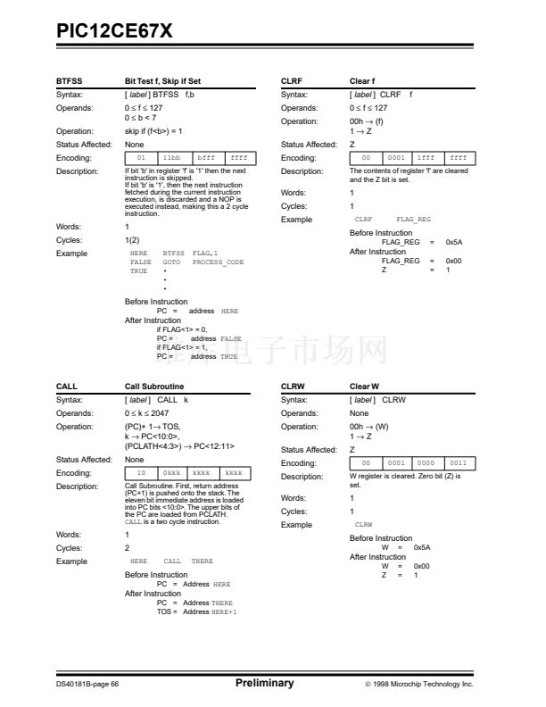
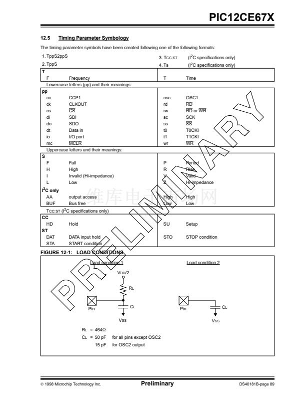
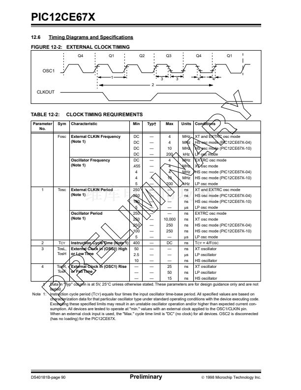
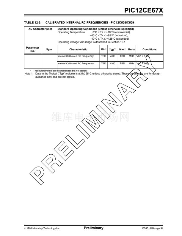
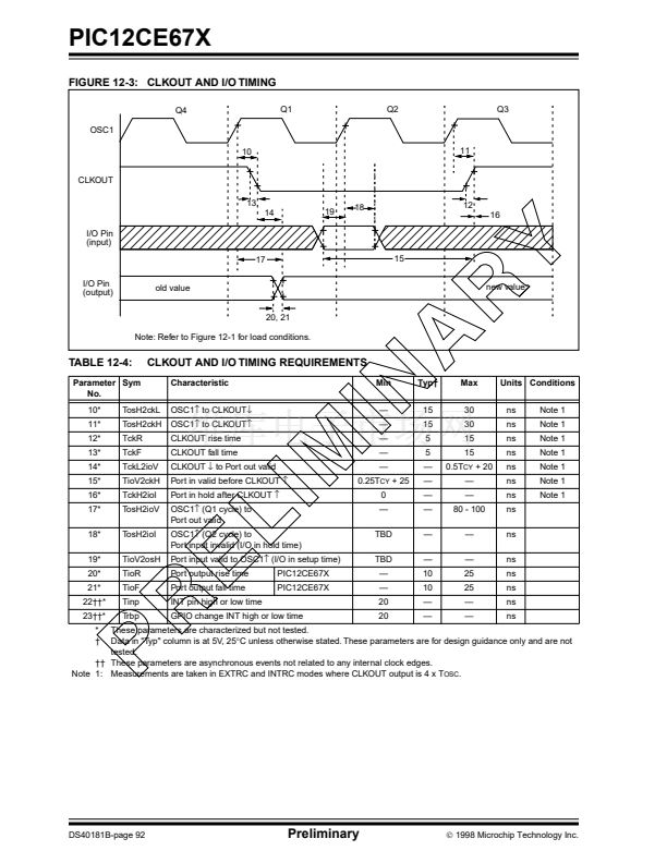
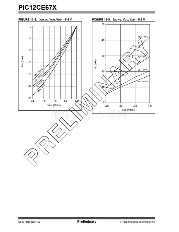
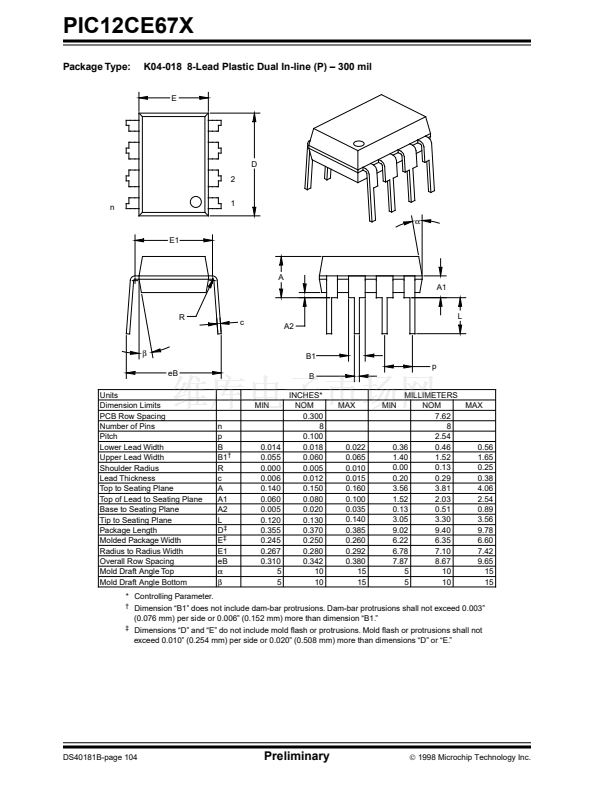
PIC12CE67X
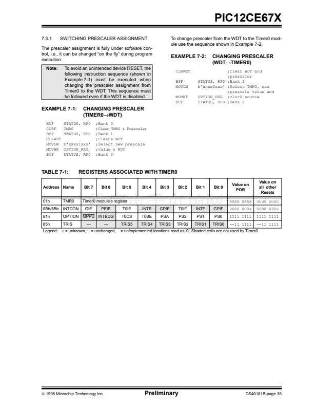
7.3.1
SWITCHING PRESCALER ASSIGNMENT
The prescaler assignment is fully under software con-
trol, i.e., it can be changed 鈥渙n the 铿倅鈥?during program
execution.
Note:
To avoid an unintended device RESET, the
following instruction sequence (shown in
Example 7-1) must be executed when
changing the prescaler assignment from
Timer0 to the WDT. This sequence must
be followed even if the WDT is disabled.
To change prescaler from the WDT to the Timer0 mod-
ule use the sequence shown in Example 7-2.
EXAMPLE 7-2:
CLRWDT
BSF
MOVLW
MOVWF
BCF
CHANGING PRESCALER
(WDT鈫扵IMER0)
;Clear WDT and
;prescaler
STATUS, RP0 ;Bank 1
b'xxxx0xxx' ;Select TMR0, new
;prescale value and
OPTION_REG ;clock source
STATUS, RP0 ;Bank 0
EXAMPLE 7-1:
BCF
CLRF
BSF
CLRWDT
MOVLW
MOVWF
BCF
CHANGING PRESCALER
(TIMER0鈫扺DT)
;Bank 0
;Clear TMR0 & Prescaler
;Bank 1
;Clears WDT
;Select new prescale
;value & WDT
;Bank 0
STATUS, RP0
TMR0
STATUS, RP0
b'xxxx1xxx'
OPTION_REG
STATUS, RP0
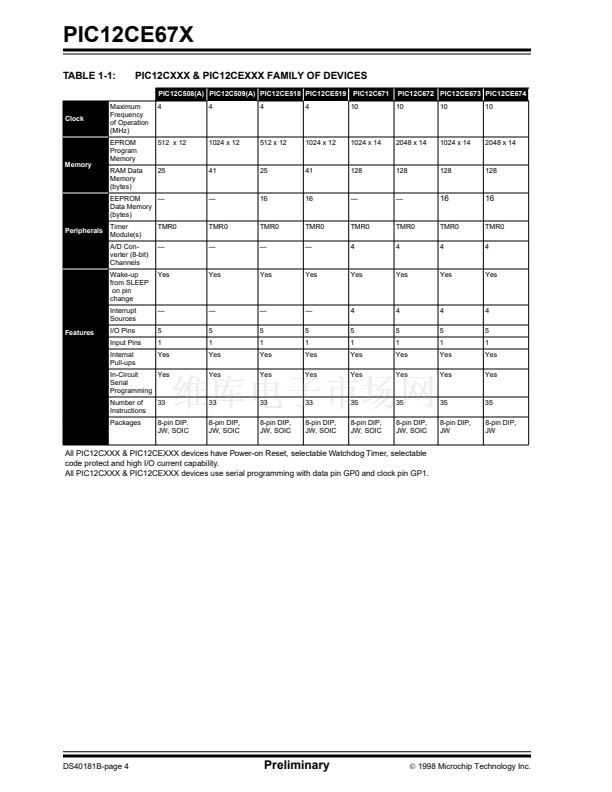
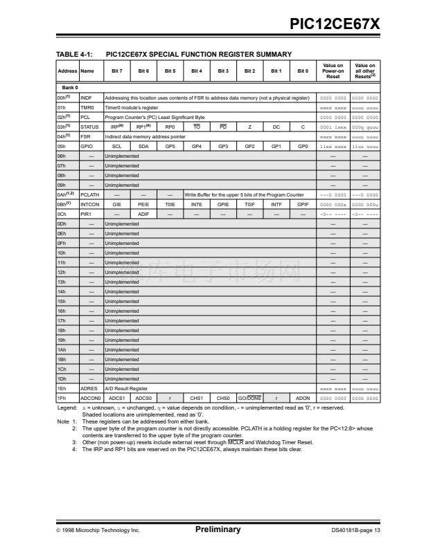
TABLE 7-1:
Address Name
01h
0Bh/8Bh
81h
85h
TMR0
REGISTERS ASSOCIATED WITH TIMER0
Bit 7
Bit 6
Bit 5
Bit 4
Bit 3
Bit 2
Bit 1
Bit 0
Value on
POR
xxxx xxxx
INTE
T0SE
TRIS4
GPIE
PSA
TRIS3
T0IF
PS2
TRIS2
INTF
PS1
TRIS1
GPIF
PS0
TRIS0
0000 000x
1111 1111
--11 1111
Value on
all other
Resets
uuuu uuuu
0000 000u
1111 1111
--11 1111
Timer0 module鈥檚 register
GIE
PEIE
T0IE
T0CS
TRIS5
INTCON
OPTION GPPU INTEDG
TRIS
鈥?/div>
鈥?/div>
Legend:
x
= unknown,
u
= unchanged,
-
= unimplemented locations read as '0'. Shaded cells are not used by Timer0.
漏
1998 Microchip Technology Inc.
Preliminary
DS40181B-page 35


 1
1
 2
2
 3
3
 4
4
 5
5
 6
6
 7
7
 8
8
 9
9
 10
10
 11
11
 12
12
 13
13
 14
14
 15
15
 16
16
 17
17
 18
18
 19
19
 20
20
 21
21
 22
22
 23
23
 24
24
 25
25
 26
26
 27
27
 28
28
 29
29
 30
30
 31
31
 32
32
 33
33
 34
34
 35
35
 36
36
 37
37
 38
38
 39
39
 40
40
 41
41
 42
42
 43
43
 44
44
 45
45
 46
46
 47
47
 48
48
 49
49
 50
50
 51
51
 52
52
 53
53
 54
54
 55
55
 56
56
 57
57
 58
58
 59
59
 60
60
 61
61
 62
62
 63
63
 64
64
 65
65
 66
66
 67
67
 68
68
 69
69
 70
70
 71
71
 72
72
 73
73
 74
74
 75
75
 76
76
 77
77
 78
78
 79
79
 80
80
 81
81
 82
82
 83
83
 84
84
 85
85
 86
86
 87
87
 88
88
 89
89
 90
90
 91
91
 92
92
 93
93
 94
94
 95
95
 96
96
 97
97
 98
98
 99
99
 100
100
 101
101
 102
102
 103
103
 104
104
 105
105
 106
106
 107
107
 108
108
 109
109
 110
110
 111
111
 112
112
 113
113
 114
114
 115
115
 116
116
