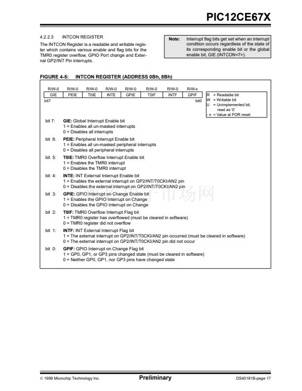
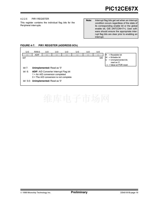
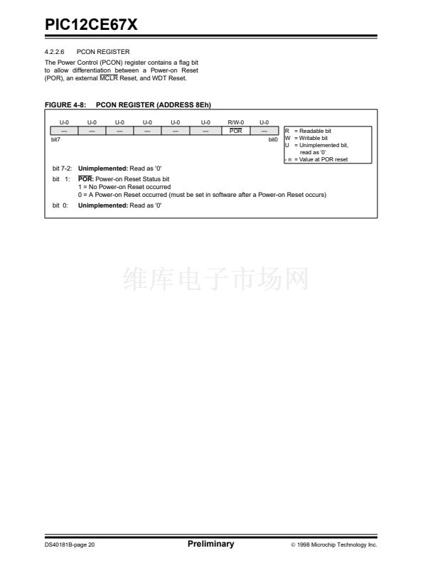
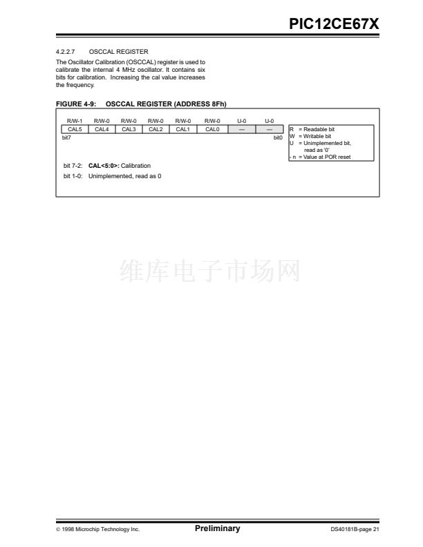
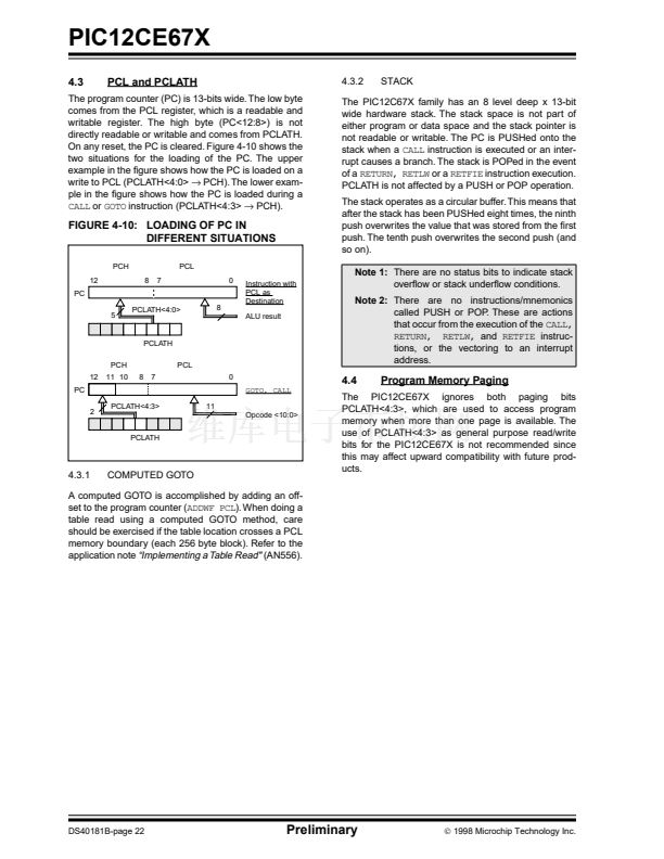
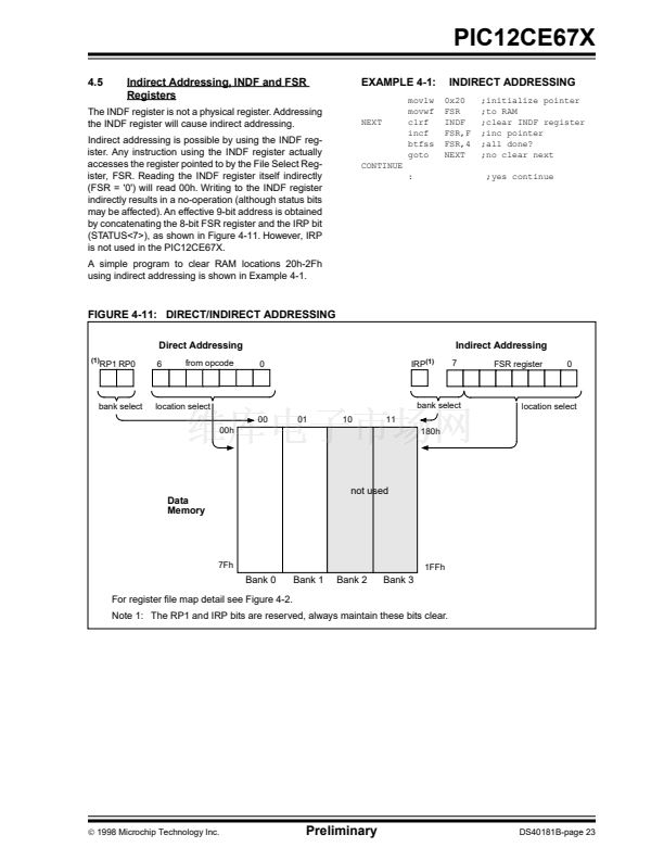
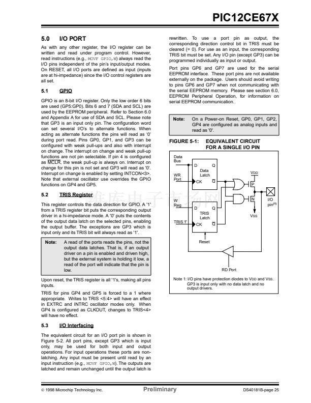
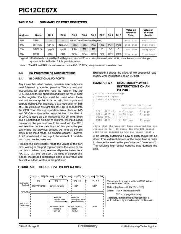
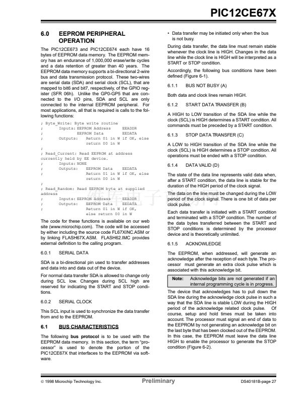
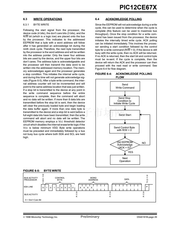
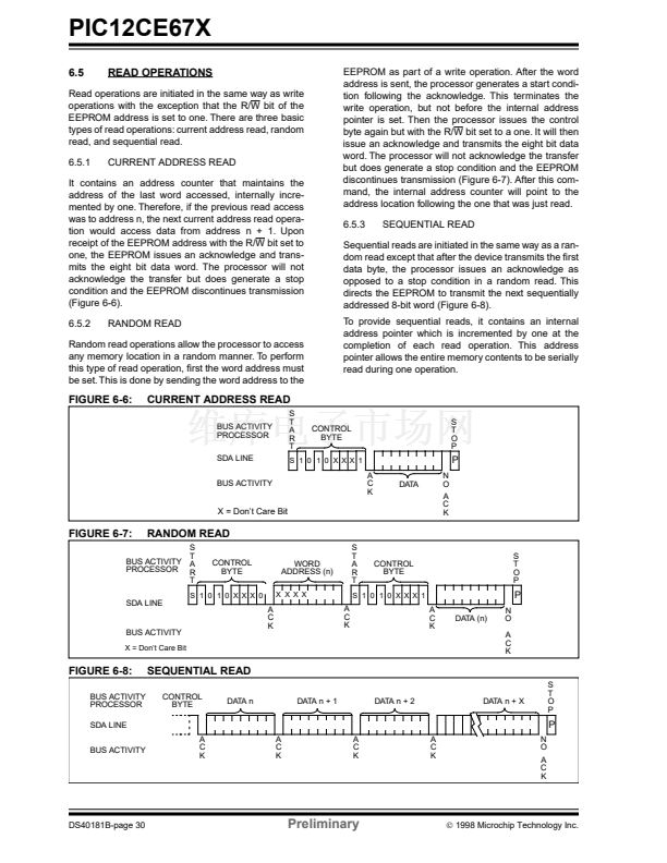
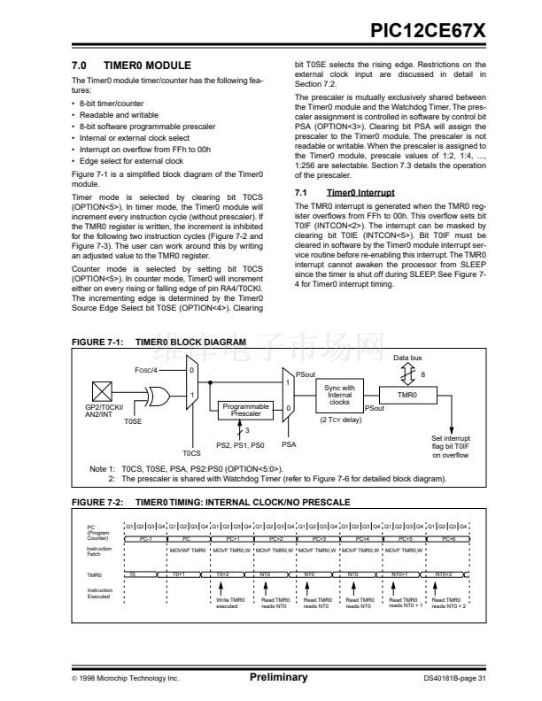
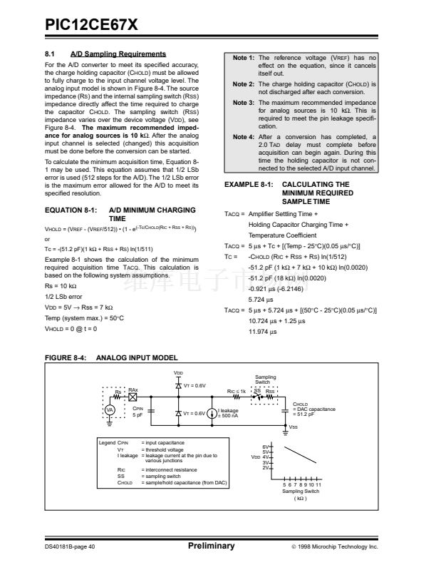
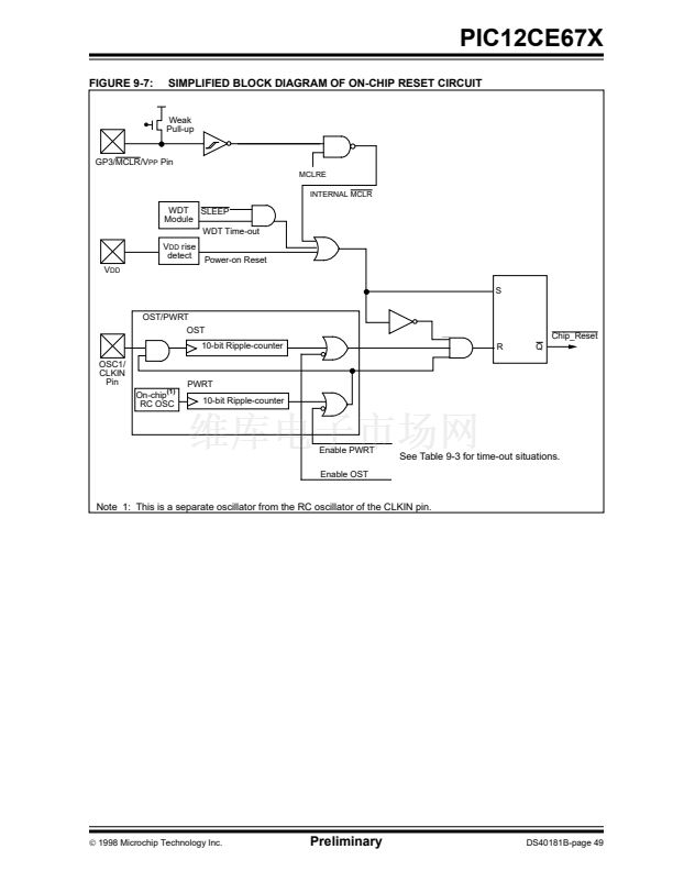
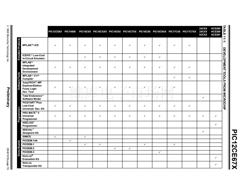
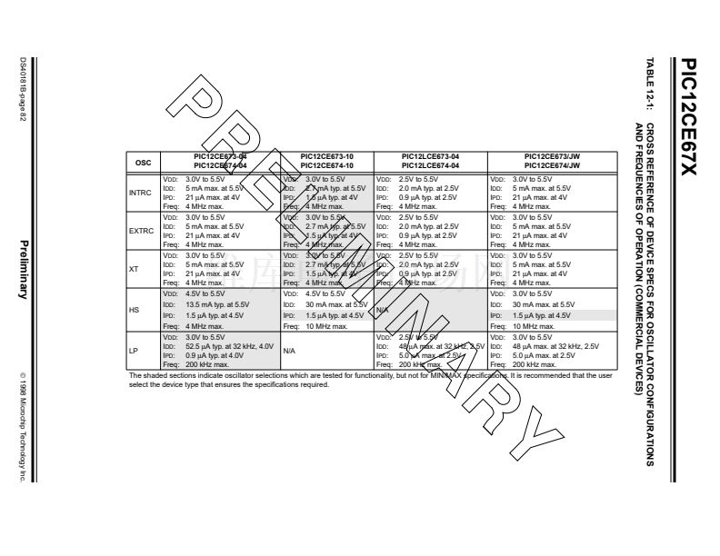
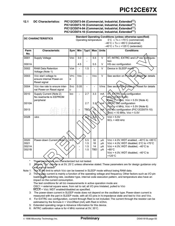
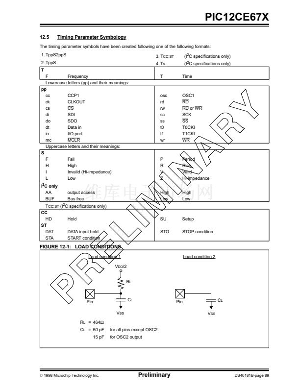
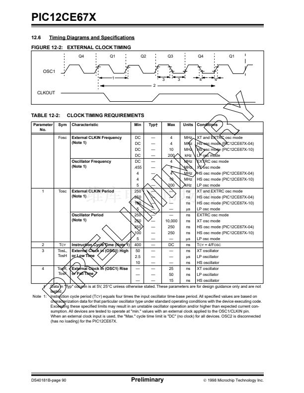
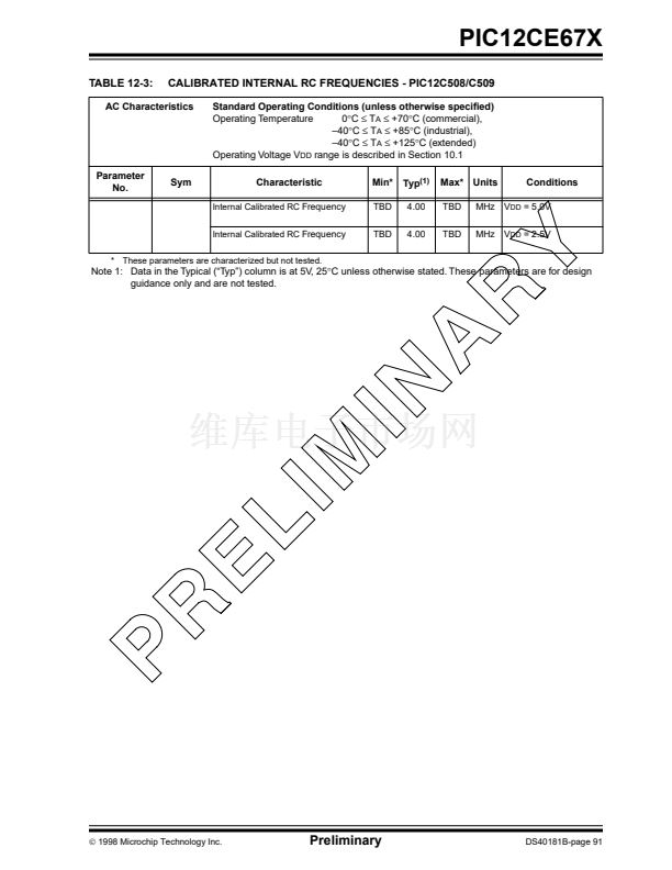
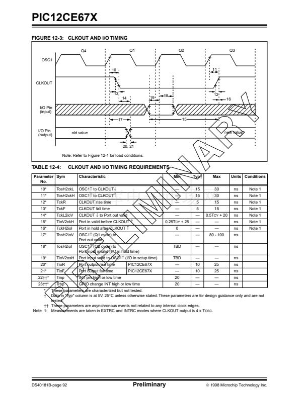
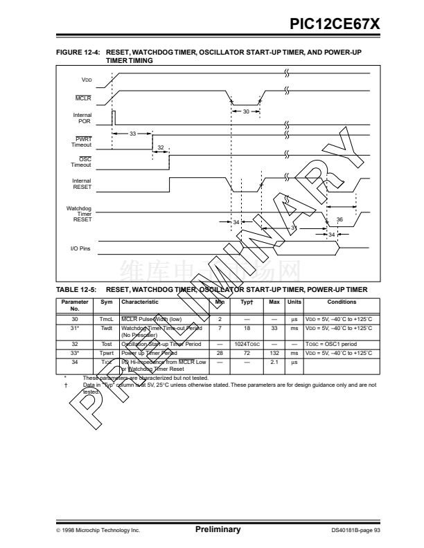
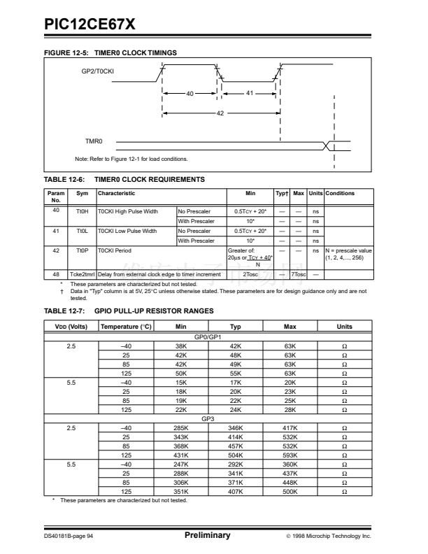
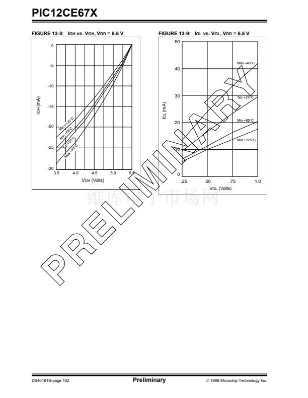
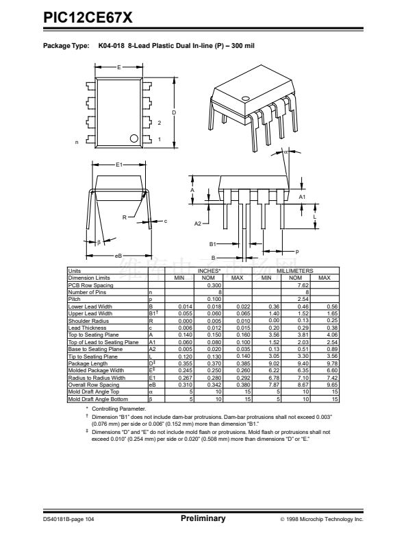
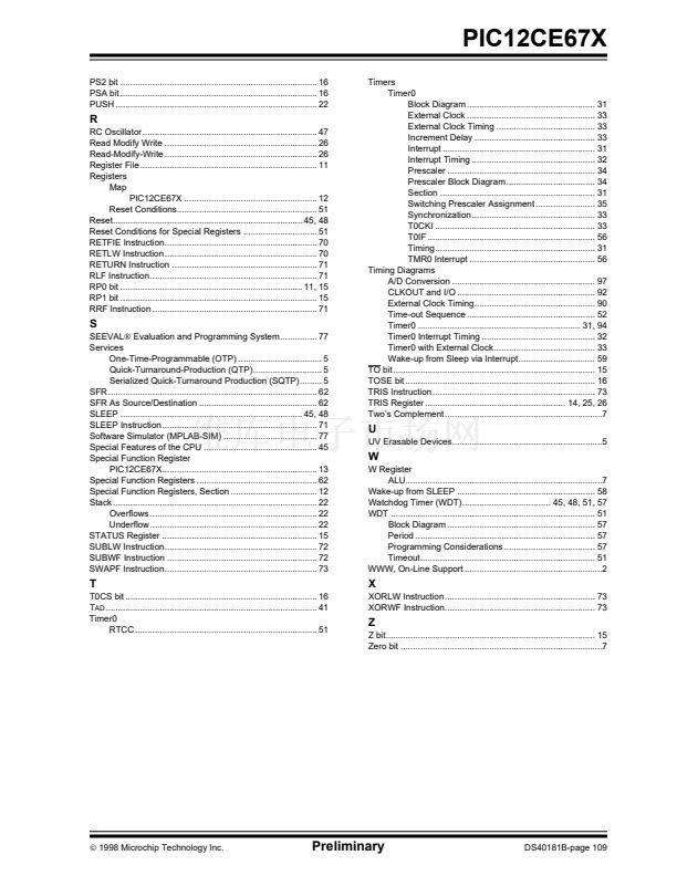
PIC12CE67X
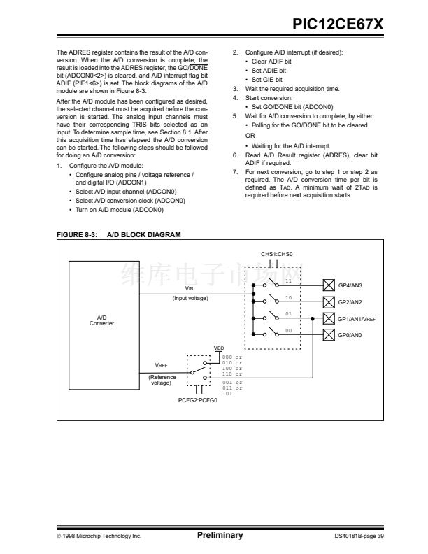
The ADRES register contains the result of the A/D con-
version. When the A/D conversion is complete, the
result is loaded into the ADRES register, the GO/DONE
bit (ADCON0<2>) is cleared, and A/D interrupt 铿俛g bit
ADIF (PIE1<6>) is set. The block diagrams of the A/D
module are shown in Figure 8-3.
After the A/D module has been con铿乬ured as desired,
the selected channel must be acquired before the con-
version is started. The analog input channels must
have their corresponding TRIS bits selected as an
input. To determine sample time, see Section 8.1. After
this acquisition time has elapsed the A/D conversion
can be started. The following steps should be followed
for doing an A/D conversion:
1.
Con铿乬ure the A/D module:
鈥?Con铿乬ure analog pins / voltage reference /
and digital I/O (ADCON1)
鈥?Select A/D input channel (ADCON0)
鈥?Select A/D conversion clock (ADCON0)
鈥?Turn on A/D module (ADCON0)
2.
Con铿乬ure A/D interrupt (if desired):
鈥?Clear ADIF bit
鈥?Set ADIE bit
鈥?Set GIE bit
Wait the required acquisition time.
Start conversion:
鈥?Set GO/DONE bit (ADCON0)
Wait for A/D conversion to complete, by either:
鈥?Polling for the GO/DONE bit to be cleared
OR
6.
7.
鈥?Waiting for the A/D interrupt
Read A/D Result register (ADRES), clear bit
ADIF if required.
For next conversion, go to step 1 or step 2 as
required. The A/D conversion time per bit is
de铿乶ed as T
AD
. A minimum wait of 2T
AD
is
required before next acquisition starts.
3.
4.
5.
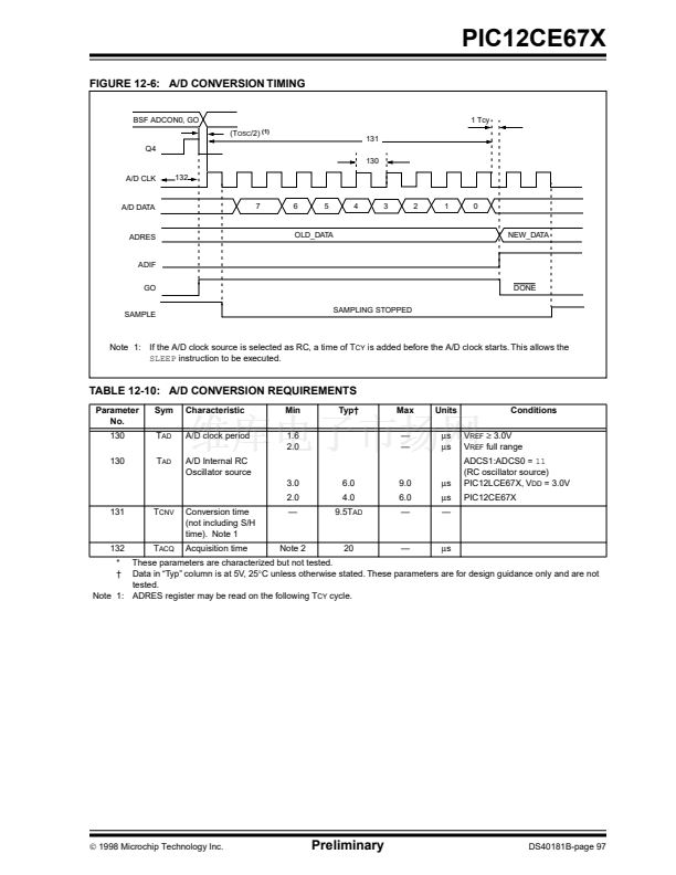
FIGURE 8-3:
A/D BLOCK DIAGRAM
CHS1:CHS0
11
V
IN
(Input voltage)
10
GP2/AN2
01
GP1/AN1/V
REF
00
V
DD
V
REF
(Reference
voltage)
PCFG2:PCFG0
000
010
100
110
001
011
101
or
or
or
or
or
or
GP0/AN0
GP4/AN3
A/D
Converter
漏
1998 Microchip Technology Inc.
Preliminary
DS40181B-page 39


 1
1
 2
2
 3
3
 4
4
 5
5
 6
6
 7
7
 8
8
 9
9
 10
10
 11
11
 12
12
 13
13
 14
14
 15
15
 16
16
 17
17
 18
18
 19
19
 20
20
 21
21
 22
22
 23
23
 24
24
 25
25
 26
26
 27
27
 28
28
 29
29
 30
30
 31
31
 32
32
 33
33
 34
34
 35
35
 36
36
 37
37
 38
38
 39
39
 40
40
 41
41
 42
42
 43
43
 44
44
 45
45
 46
46
 47
47
 48
48
 49
49
 50
50
 51
51
 52
52
 53
53
 54
54
 55
55
 56
56
 57
57
 58
58
 59
59
 60
60
 61
61
 62
62
 63
63
 64
64
 65
65
 66
66
 67
67
 68
68
 69
69
 70
70
 71
71
 72
72
 73
73
 74
74
 75
75
 76
76
 77
77
 78
78
 79
79
 80
80
 81
81
 82
82
 83
83
 84
84
 85
85
 86
86
 87
87
 88
88
 89
89
 90
90
 91
91
 92
92
 93
93
 94
94
 95
95
 96
96
 97
97
 98
98
 99
99
 100
100
 101
101
 102
102
 103
103
 104
104
 105
105
 106
106
 107
107
 108
108
 109
109
 110
110
 111
111
 112
112
 113
113
 114
114
 115
115
 116
116
