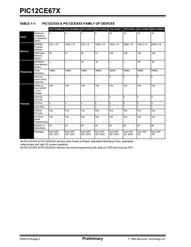
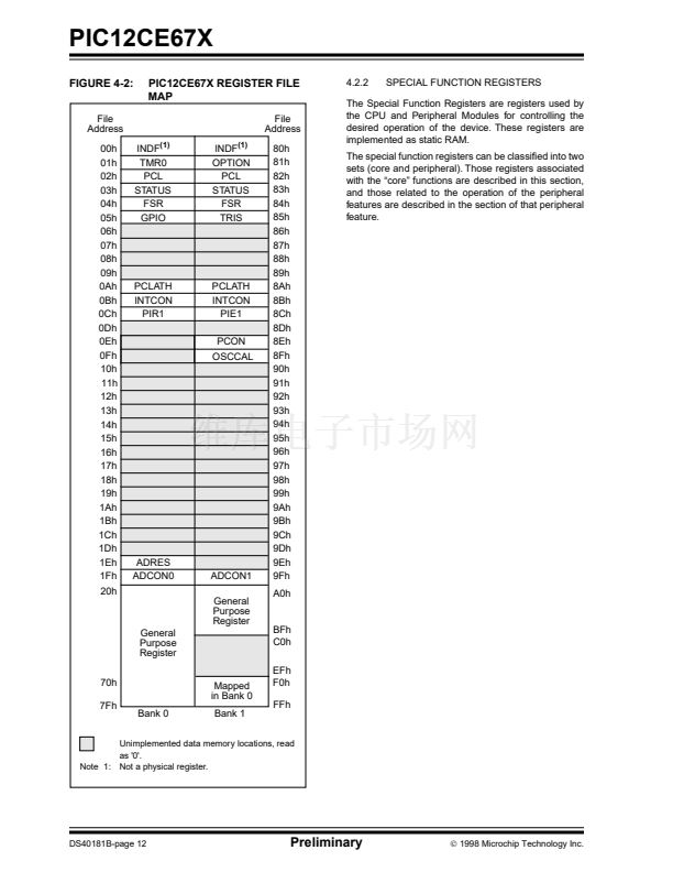
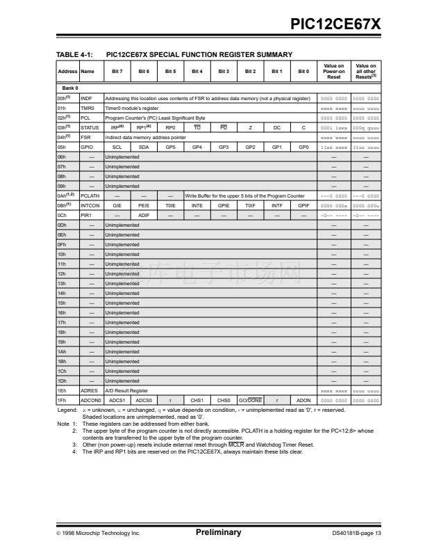
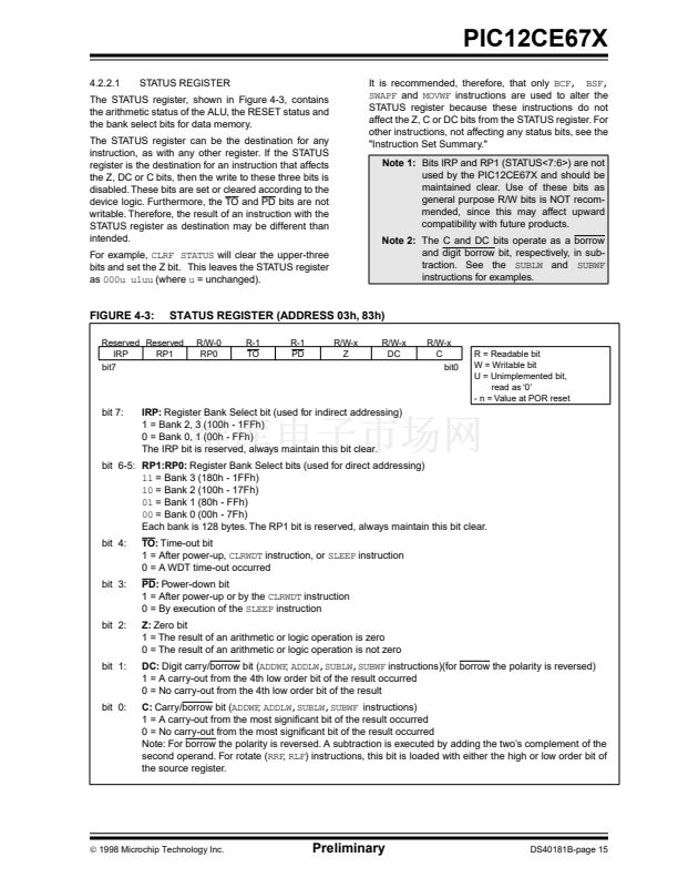
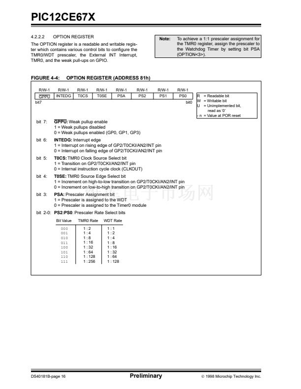
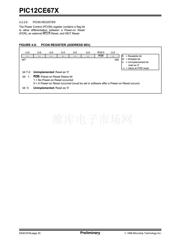
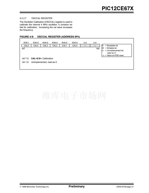
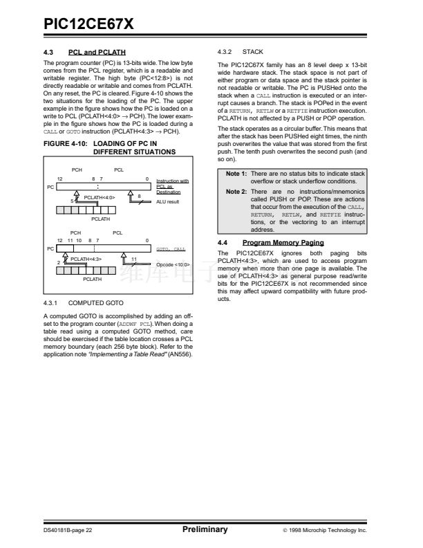
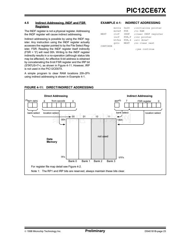
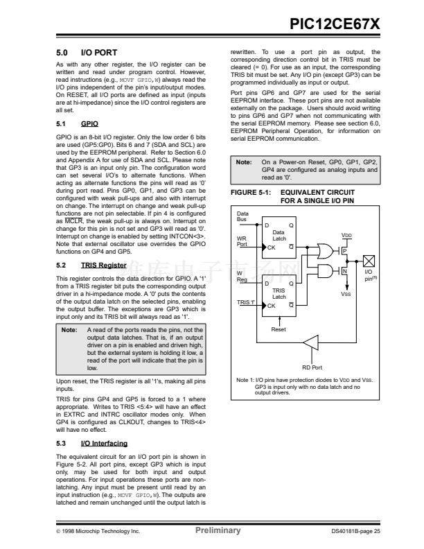
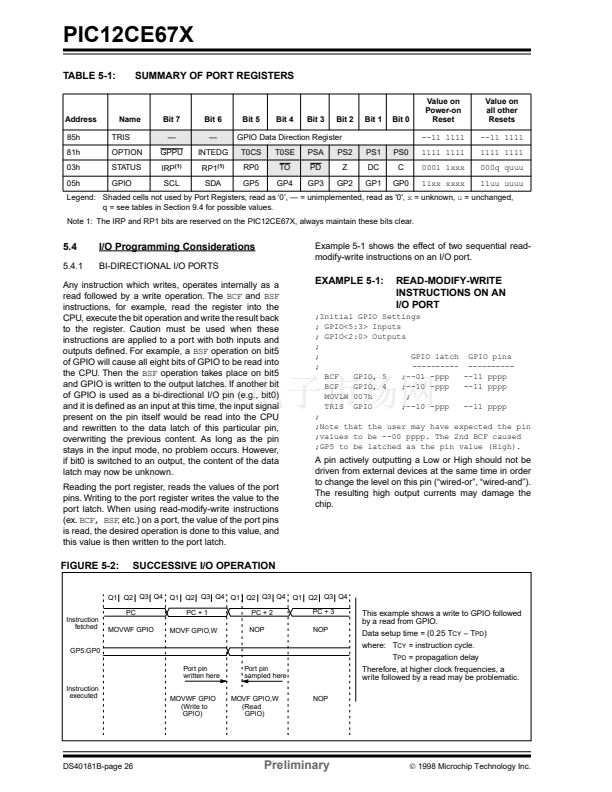
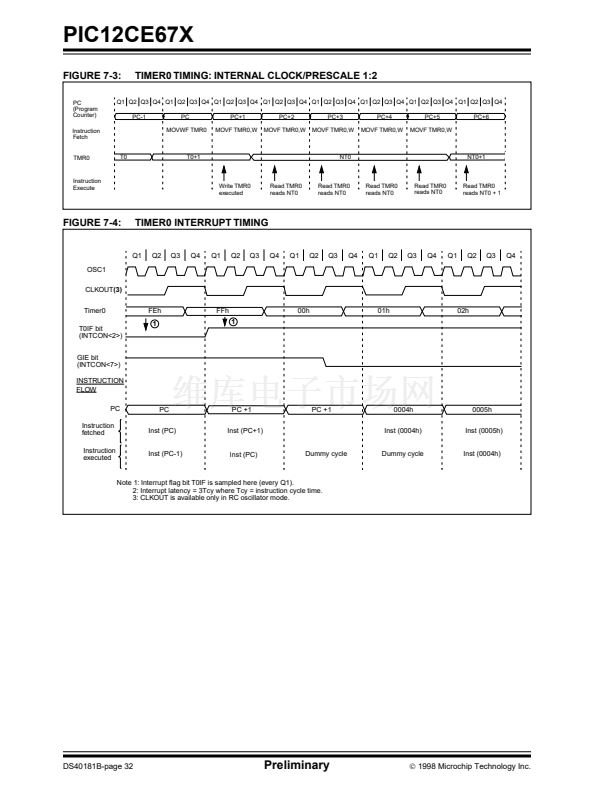
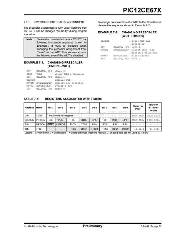
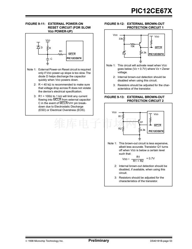
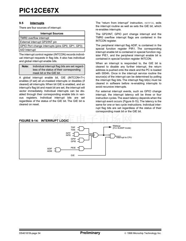
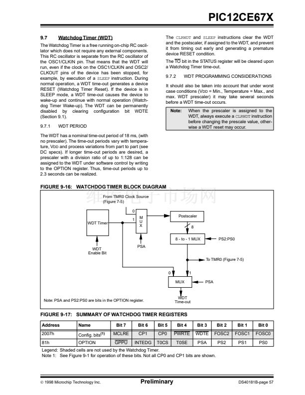
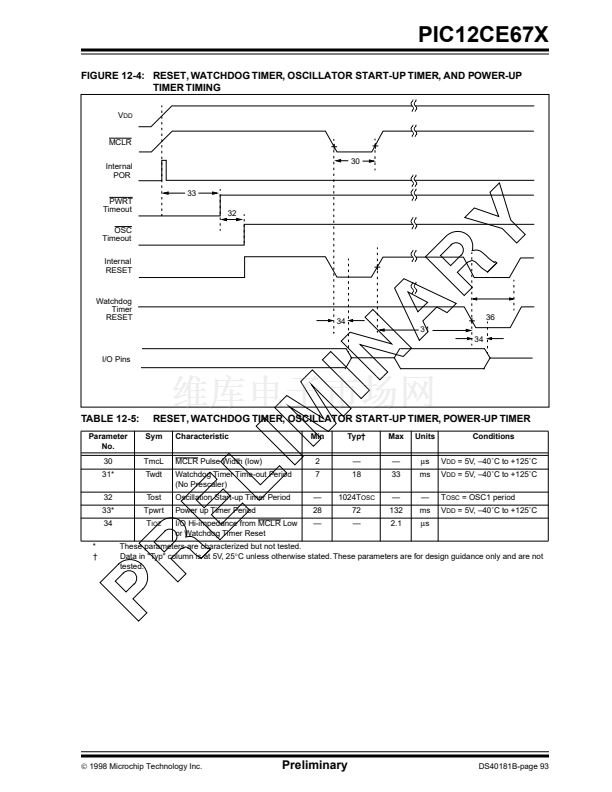
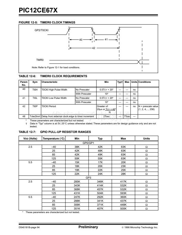
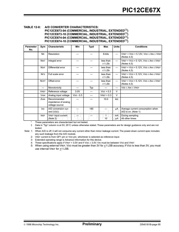
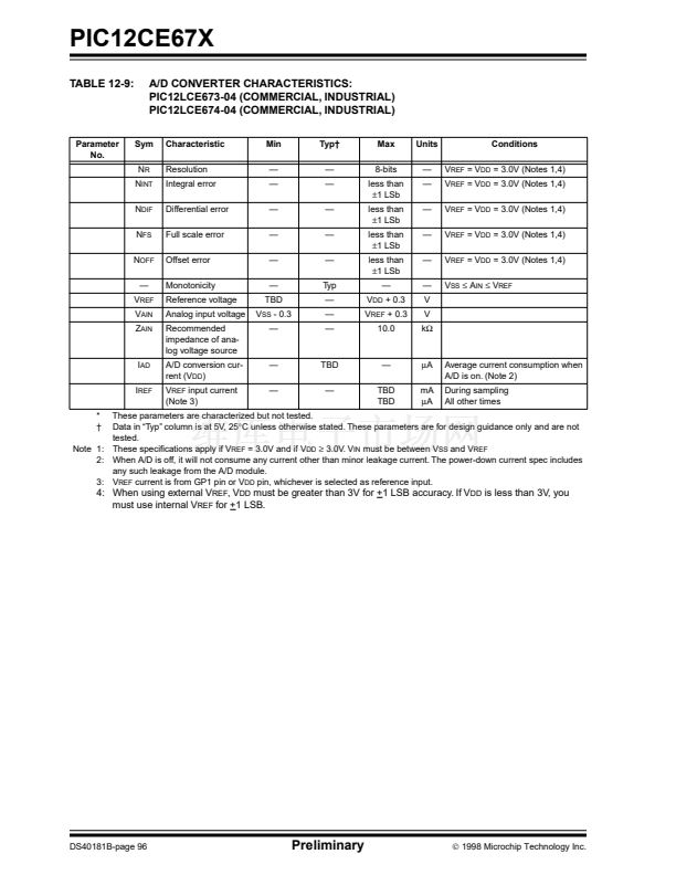
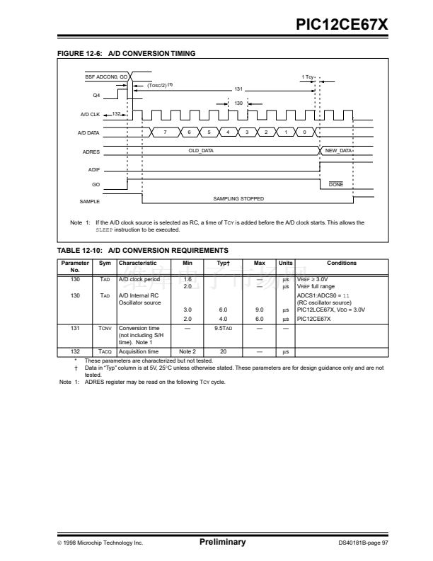
PIC12CE67X
8.1
A/D Sampling Requirements
For the A/D converter to meet its speci铿乪d accuracy,
the charge holding capacitor (C
HOLD
) must be allowed
to fully charge to the input channel voltage level. The
analog input model is shown in Figure 8-4. The source
impedance (R
S
) and the internal sampling switch (R
SS
)
impedance directly affect the time required to charge
the capacitor C
HOLD
. The sampling switch (R
SS
)
impedance varies over the device voltage (V
DD
), see
Figure 8-4.
The maximum recommended imped-
ance for analog sources is 10 k鈩?
After the analog
input channel is selected (changed) this acquisition
must be done before the conversion can be started.
To calculate the minimum acquisition time, Equation 8-
1 may be used. This equation assumes that 1/2 LSb
error is used (512 steps for the A/D). The 1/2 LSb error
is the maximum error allowed for the A/D to meet its
speci铿乪d resolution.
Note 1:
The reference voltage (V
REF
) has no
effect on the equation, since it cancels
itself out.
Note 2:
The charge holding capacitor (C
HOLD
) is
not discharged after each conversion.
Note 3:
The maximum recommended impedance
for analog sources is 10 k鈩? This is
required to meet the pin leakage speci铿?
cation.
Note 4:
After a conversion has completed, a
2.0 T
AD
delay must complete before
acquisition can begin again. During this
time the holding capacitor is not con-
nected to the selected A/D input channel.
EXAMPLE 8-1:
CALCULATING THE
MINIMUM REQUIRED
SAMPLE TIME
EQUATION 8-1:
A/D MINIMUM CHARGING
TIME
T
ACQ
= Ampli铿乪r Settling Time +
Holding Capacitor Charging Time +
Temperature Coef铿乧ient
T
ACQ
= 5
碌s
+ Tc + [(Temp - 25掳C)(0.05
碌s/掳C)]
T
C
=
-C
HOLD
(R
IC
+ R
SS
+ R
S
) ln(1/512)
-51.2 pF (1 k鈩?+ 7 k鈩?+ 10 k鈩? ln(0.0020)
-51.2 pF (18 k鈩? ln(0.0020)
-0.921
碌s
(-6.2146)
5.724
碌s
T
ACQ
= 5
碌s
+ 5.724
碌s
+ [(50掳C - 25掳C)(0.05
碌s/掳C)]
10.724
碌s
+ 1.25
碌s
11.974
碌s
V
HOLD
= (V
REF
- (V
REF
/512)) 鈥?(1 - e
(-Tc/C
HOLD
(R
IC
+ R
SS
+ R
S
))
)
or
Tc = -(51.2 pF)(1 k鈩?+ R
SS
+ R
S
) ln(1/511)
Example 8-1 shows the calculation of the minimum
required acquisition time T
ACQ
. This calculation is
based on the following system assumptions.
Rs = 10 k
鈩?/div>
1/2 LSb error
V
DD
= 5V
鈫?/div>
Rss = 7 k
鈩?/div>
Temp (system max.) = 50
掳
C
V
HOLD
= 0 @ t = 0
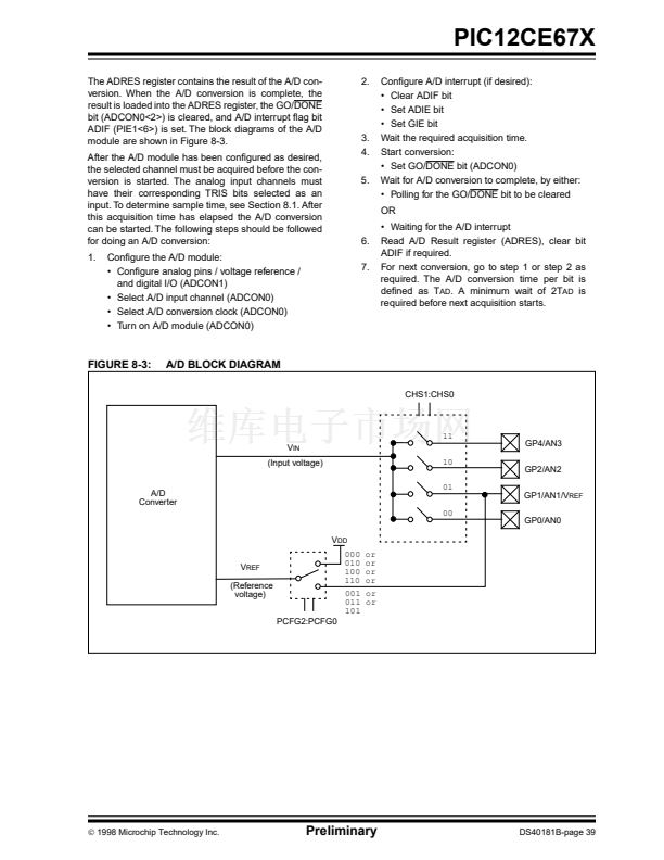
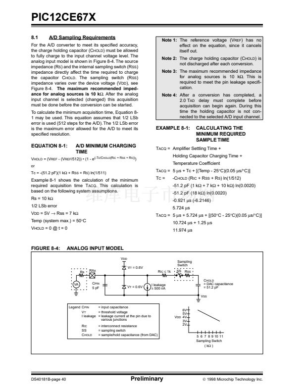
FIGURE 8-4:
ANALOG INPUT MODEL
V
DD
V
T
= 0.6V
R
IC
鈮?/div>
1k
Sampling
Switch
SS R
SS
C
HOLD
= DAC capacitance
= 51.2 pF
V
SS
Legend C
PIN
= input capacitance
V
T
= threshold voltage
I leakage = leakage current at the pin due to
various junctions
R
IC
SS
C
HOLD
= interconnect resistance
= sampling switch
= sample/hold capacitance (from DAC)
Rs
RAx
VA
C
PIN
5 pF
V
T
= 0.6V
I leakage
卤
500 nA
V
DD
6V
5V
4V
3V
2V
5 6 7 8 9 10 11
Sampling Switch
( k鈩?)
DS40181B-page 40
Preliminary
漏
1998 Microchip Technology Inc.


 1
1
 2
2
 3
3
 4
4
 5
5
 6
6
 7
7
 8
8
 9
9
 10
10
 11
11
 12
12
 13
13
 14
14
 15
15
 16
16
 17
17
 18
18
 19
19
 20
20
 21
21
 22
22
 23
23
 24
24
 25
25
 26
26
 27
27
 28
28
 29
29
 30
30
 31
31
 32
32
 33
33
 34
34
 35
35
 36
36
 37
37
 38
38
 39
39
 40
40
 41
41
 42
42
 43
43
 44
44
 45
45
 46
46
 47
47
 48
48
 49
49
 50
50
 51
51
 52
52
 53
53
 54
54
 55
55
 56
56
 57
57
 58
58
 59
59
 60
60
 61
61
 62
62
 63
63
 64
64
 65
65
 66
66
 67
67
 68
68
 69
69
 70
70
 71
71
 72
72
 73
73
 74
74
 75
75
 76
76
 77
77
 78
78
 79
79
 80
80
 81
81
 82
82
 83
83
 84
84
 85
85
 86
86
 87
87
 88
88
 89
89
 90
90
 91
91
 92
92
 93
93
 94
94
 95
95
 96
96
 97
97
 98
98
 99
99
 100
100
 101
101
 102
102
 103
103
 104
104
 105
105
 106
106
 107
107
 108
108
 109
109
 110
110
 111
111
 112
112
 113
113
 114
114
 115
115
 116
116
