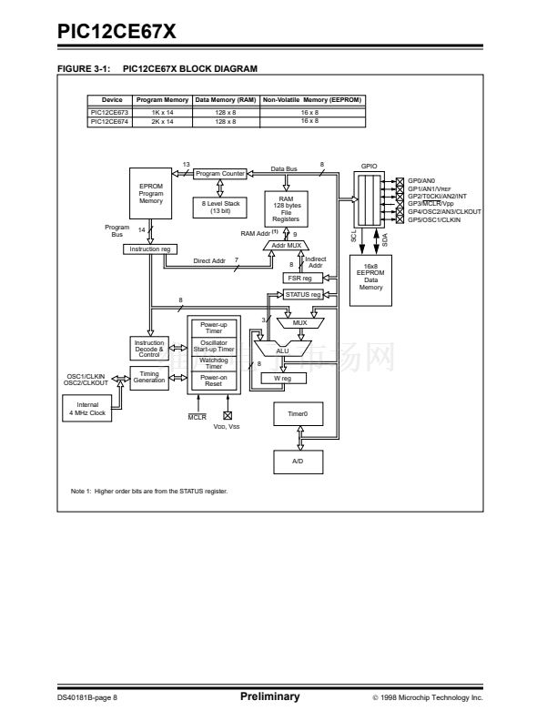
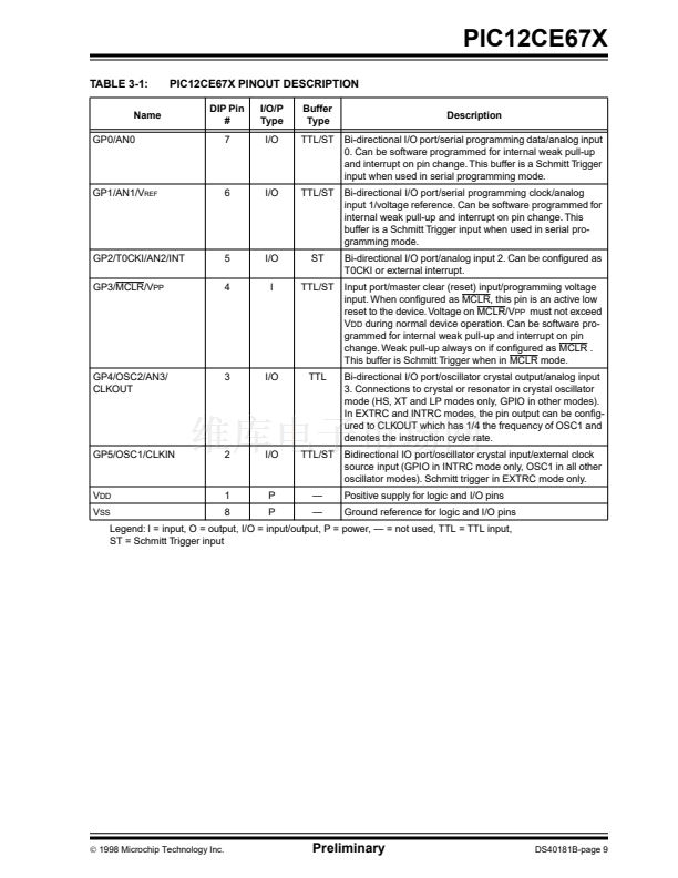
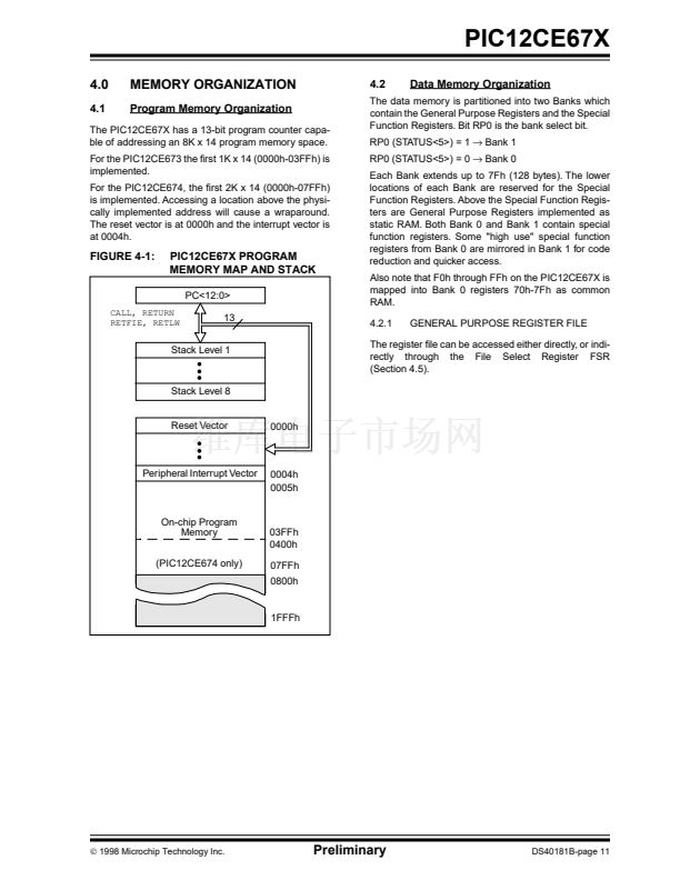
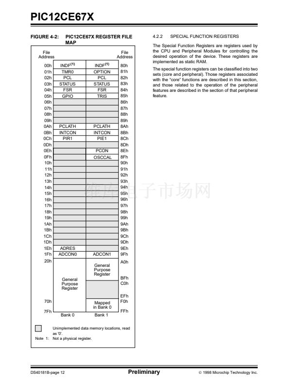
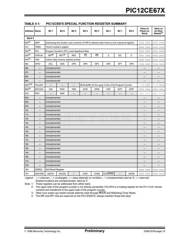
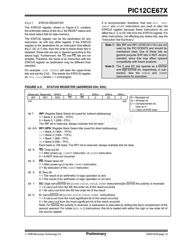
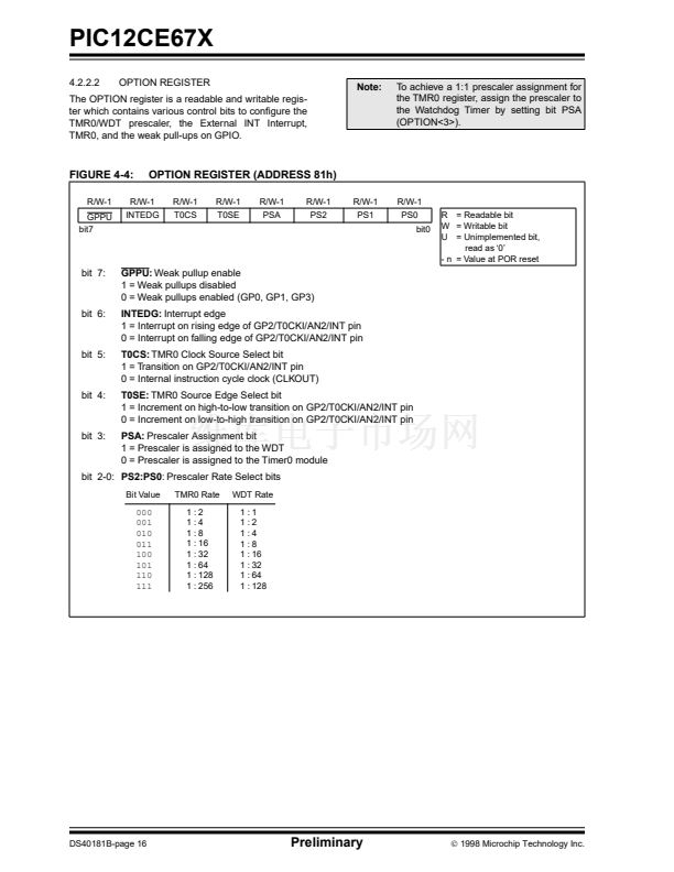
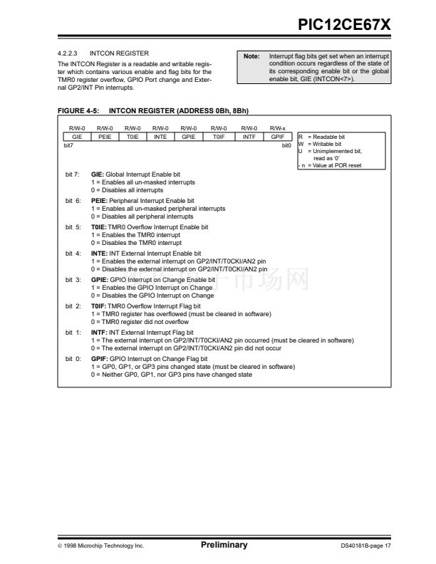
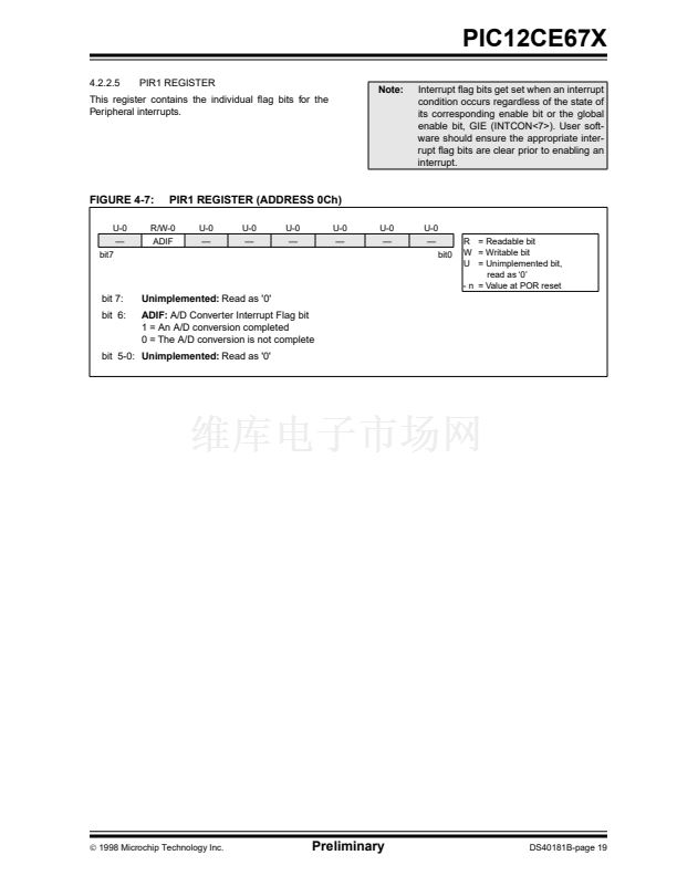
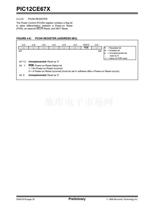
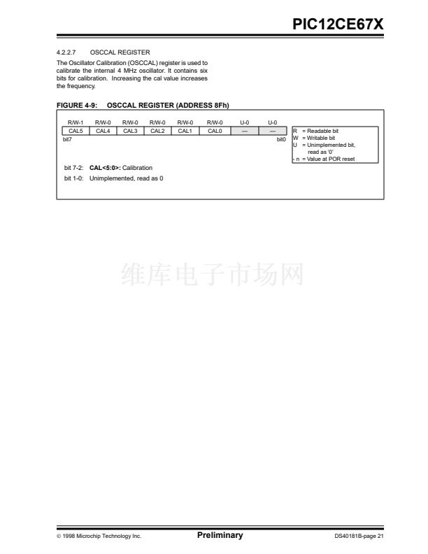
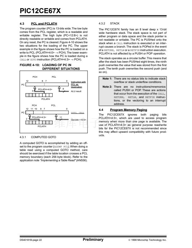
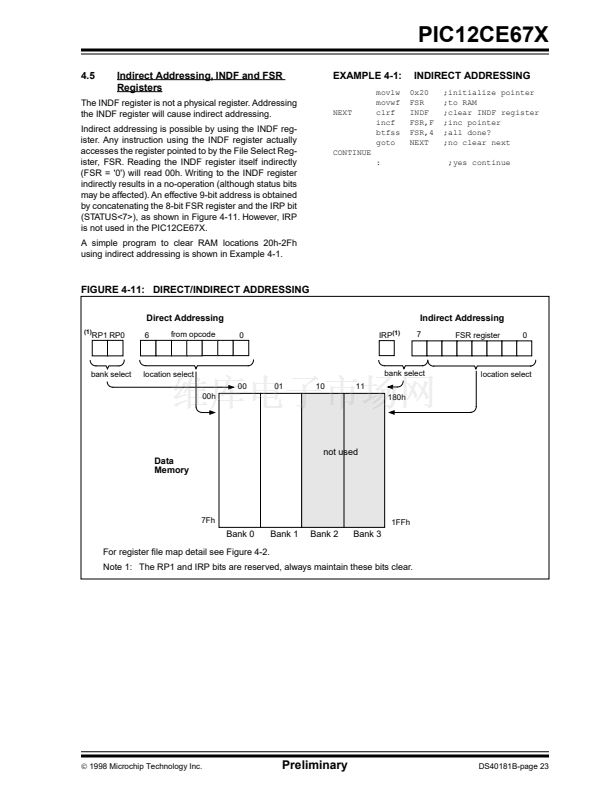
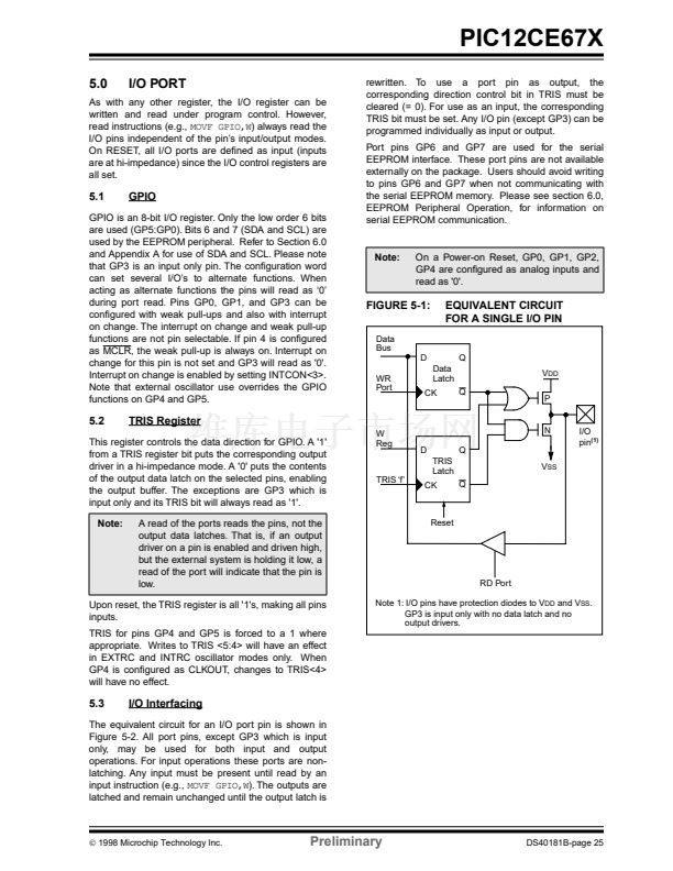
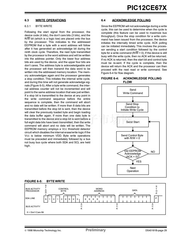
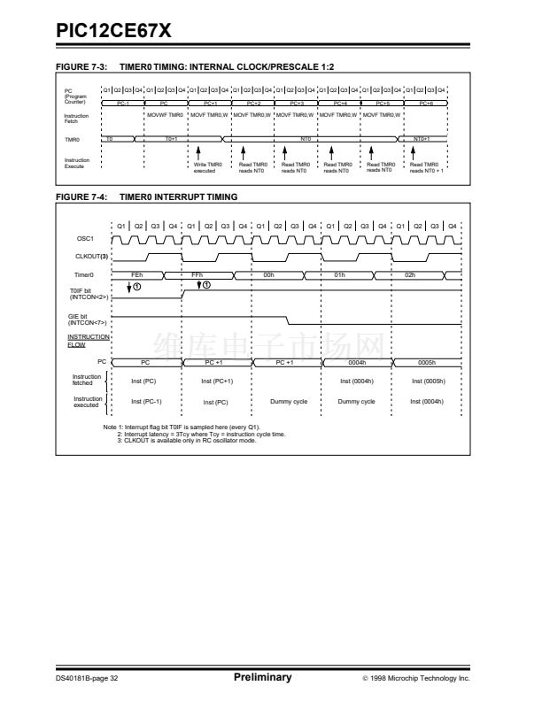
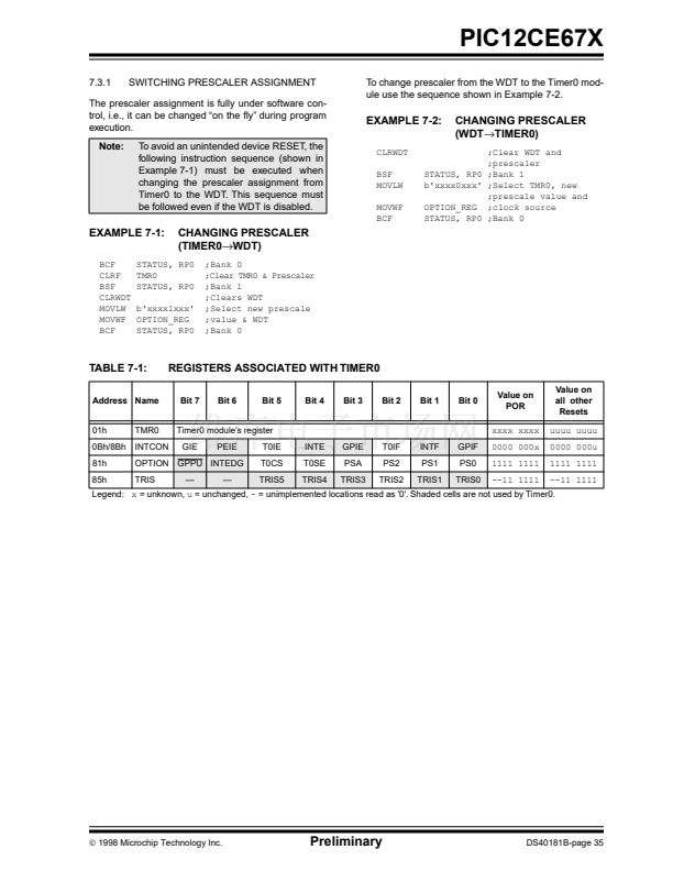
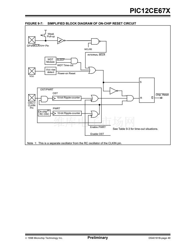
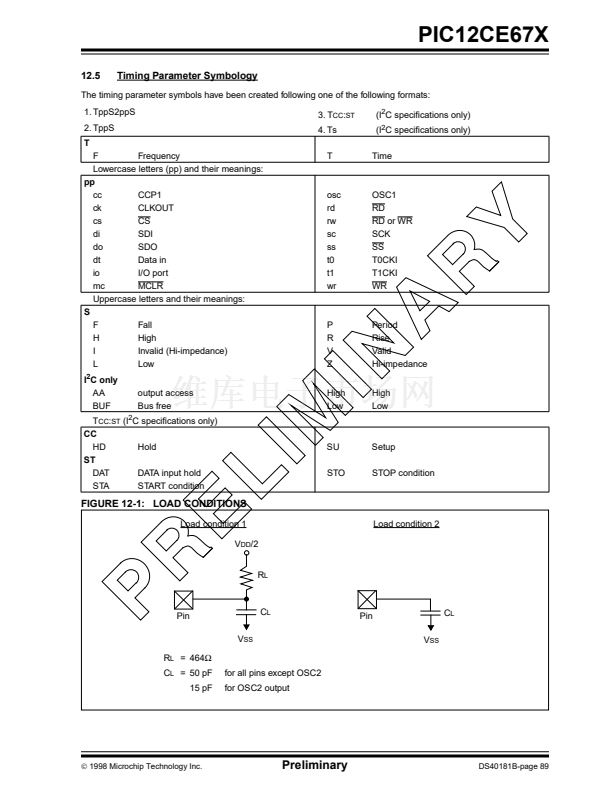
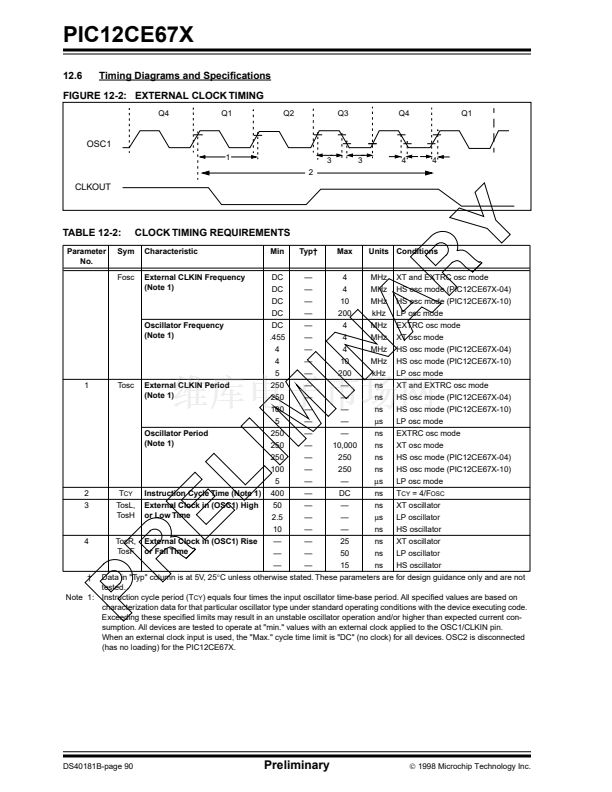
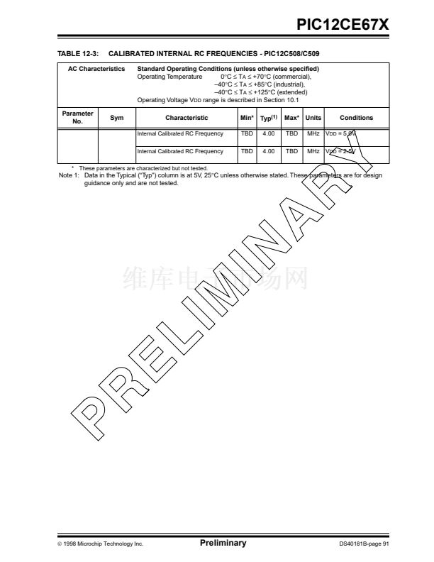
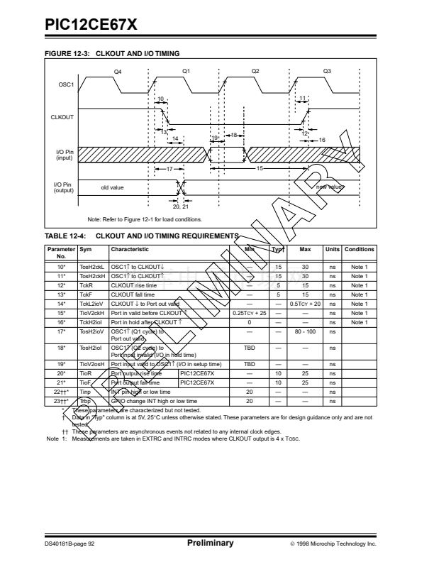
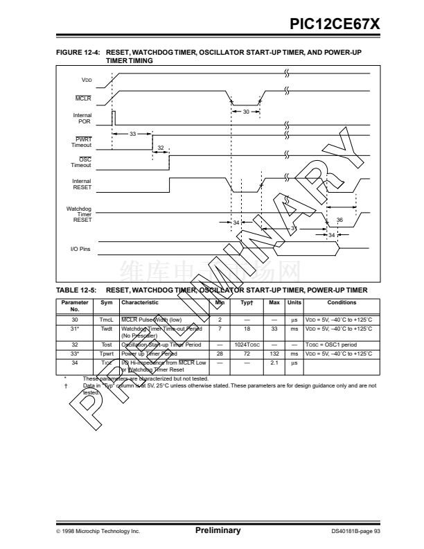
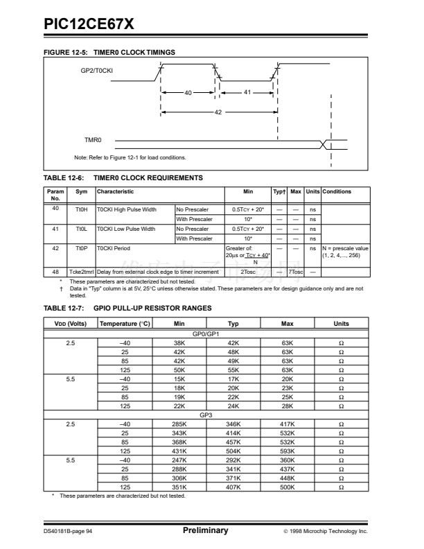
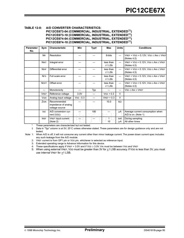
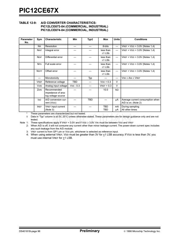
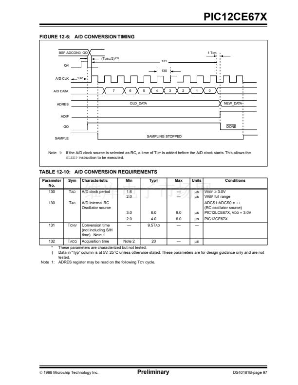
PIC12CE67X
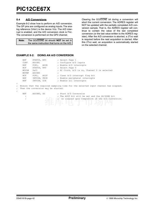
8.4
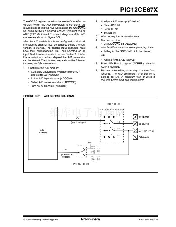
A/D Conversions
Example 8-2 show how to perform an A/D conversion.
The GP pins are con铿乬ured as analog inputs. The ana-
log reference (V
REF
) is the device V
DD
. The A/D inter-
rupt is enabled, and the A/D conversion clock is F
RC
.
The conversion is performed on the GP0 channel.
Note:
The GO/DONE bit should
NOT
be set in
the same instruction that turns on the A/D.
Clearing the GO/DONE bit during a conversion will
abort the current conversion. The ADRES register will
NOT be updated with the partially completed A/D con-
version sample. That is, the ADRES register will con-
tinue to contain the value of the last completed
conversion (or the last value written to the ADRES reg-
ister). After the A/D conversion is aborted, a 2T
AD
wait
is required before the next acquisition is started. After
this 2T
AD
wait, an acquisition is automatically started
on the selected channel.
EXAMPLE 8-2:
BSF
CLRF
BSF
BCF
MOVLW
MOVWF
BCF
BSF
BSF
;
;
;
;
DOING AN A/D CONVERSION
RP0
ADIE
RP0
;
;
;
;
;
;
;
;
;
Select Page 1
Configure A/D inputs
Enable A/D interrupts
Select Page 0
RC Clock, A/D is on, Channel 0 is selected
Clear A/D interrupt flag bit
Enable peripheral interrupts
Enable all interrupts
STATUS,
ADCON1
PIE1,
STATUS,
0xC1
ADCON0
PIR1,
INTCON,
INTCON,
ADIF
PEIE
GIE
Ensure that the required sampling time for the selected input channel has elapsed.
Then the conversion may be started.
BSF
:
:
ADCON0, GO
; Start A/D Conversion
; The ADIF bit will be set and the GO/DONE bit
; is cleared upon completion of the A/D Conversion.
DS40181B-page 42
Preliminary
漏
1998 Microchip Technology Inc.


 1
1
 2
2
 3
3
 4
4
 5
5
 6
6
 7
7
 8
8
 9
9
 10
10
 11
11
 12
12
 13
13
 14
14
 15
15
 16
16
 17
17
 18
18
 19
19
 20
20
 21
21
 22
22
 23
23
 24
24
 25
25
 26
26
 27
27
 28
28
 29
29
 30
30
 31
31
 32
32
 33
33
 34
34
 35
35
 36
36
 37
37
 38
38
 39
39
 40
40
 41
41
 42
42
 43
43
 44
44
 45
45
 46
46
 47
47
 48
48
 49
49
 50
50
 51
51
 52
52
 53
53
 54
54
 55
55
 56
56
 57
57
 58
58
 59
59
 60
60
 61
61
 62
62
 63
63
 64
64
 65
65
 66
66
 67
67
 68
68
 69
69
 70
70
 71
71
 72
72
 73
73
 74
74
 75
75
 76
76
 77
77
 78
78
 79
79
 80
80
 81
81
 82
82
 83
83
 84
84
 85
85
 86
86
 87
87
 88
88
 89
89
 90
90
 91
91
 92
92
 93
93
 94
94
 95
95
 96
96
 97
97
 98
98
 99
99
 100
100
 101
101
 102
102
 103
103
 104
104
 105
105
 106
106
 107
107
 108
108
 109
109
 110
110
 111
111
 112
112
 113
113
 114
114
 115
115
 116
116
