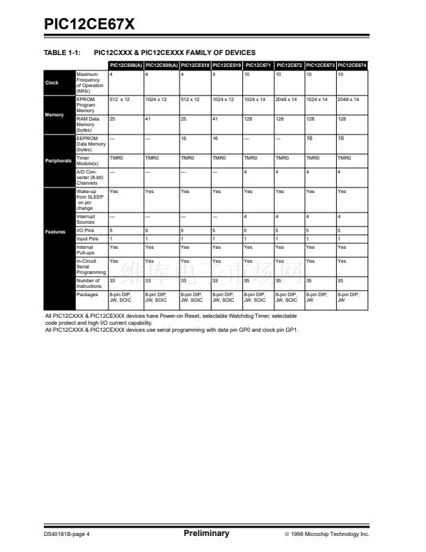
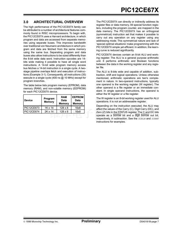
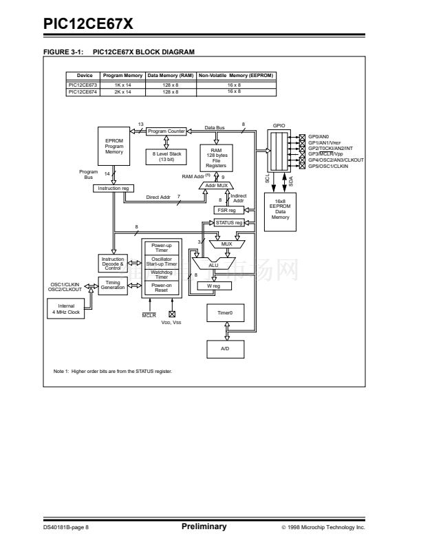
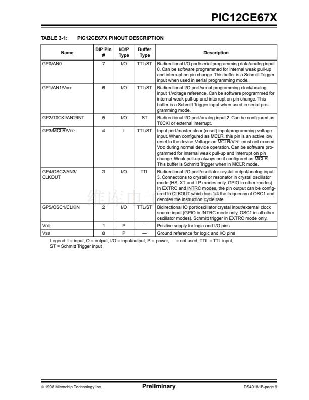
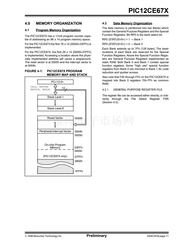
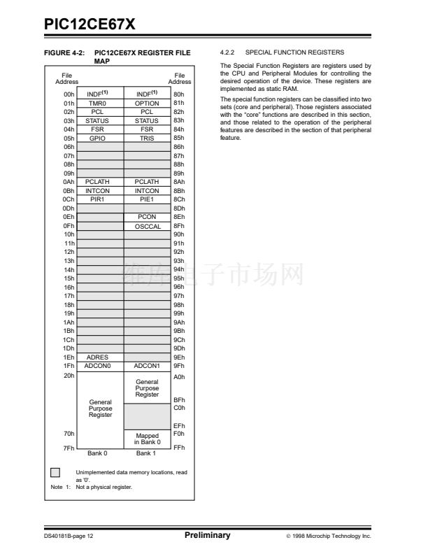
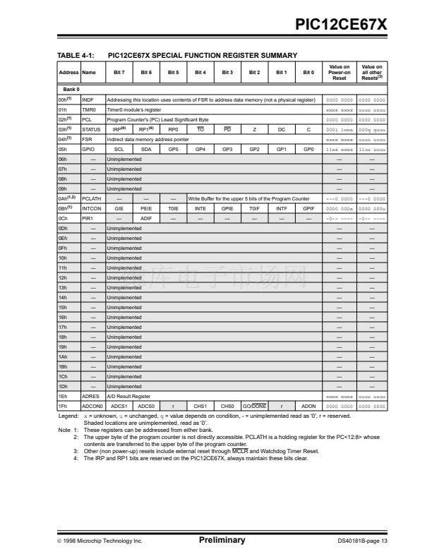
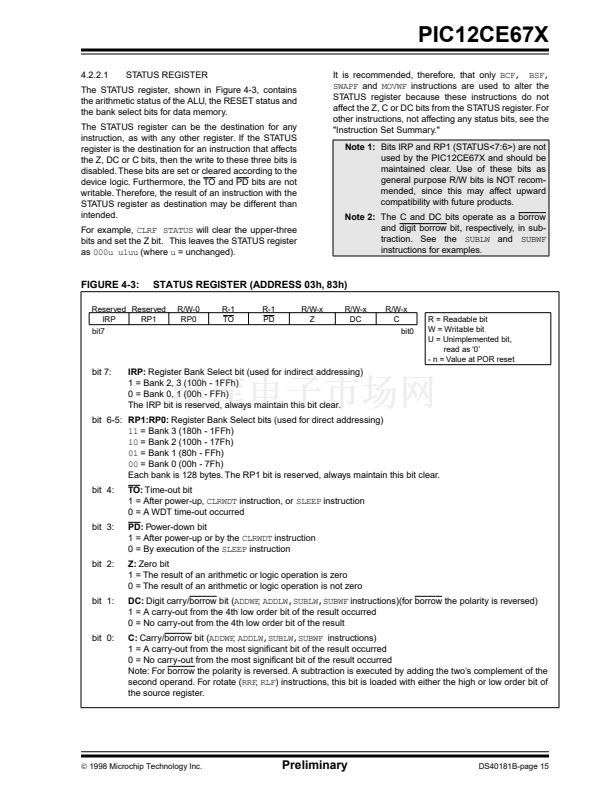
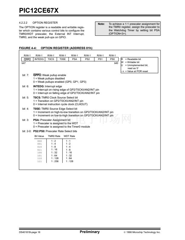
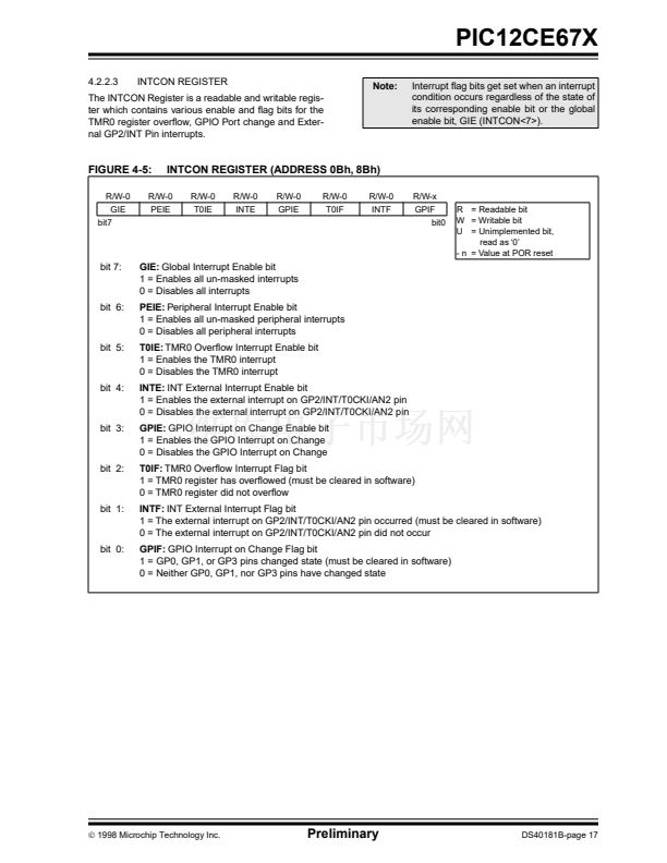
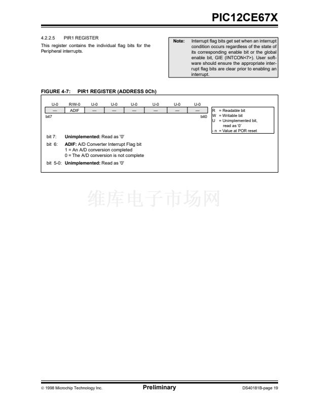
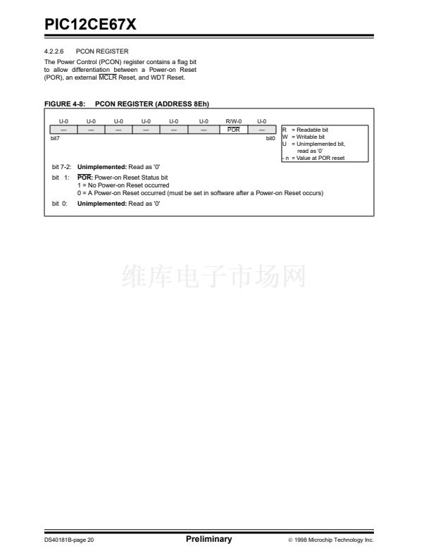
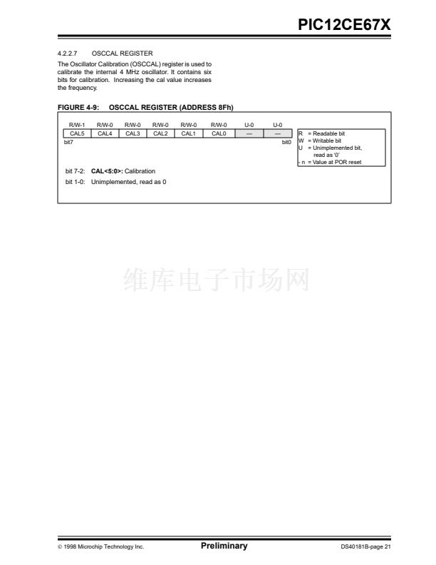
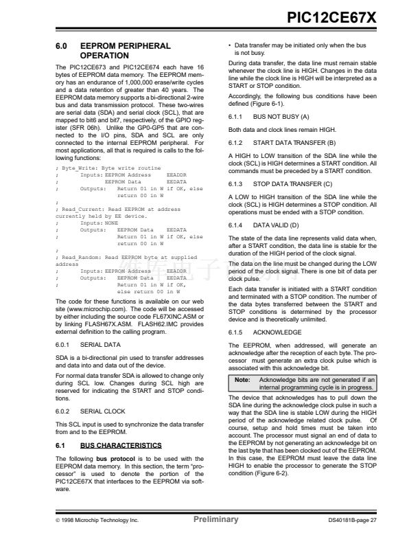
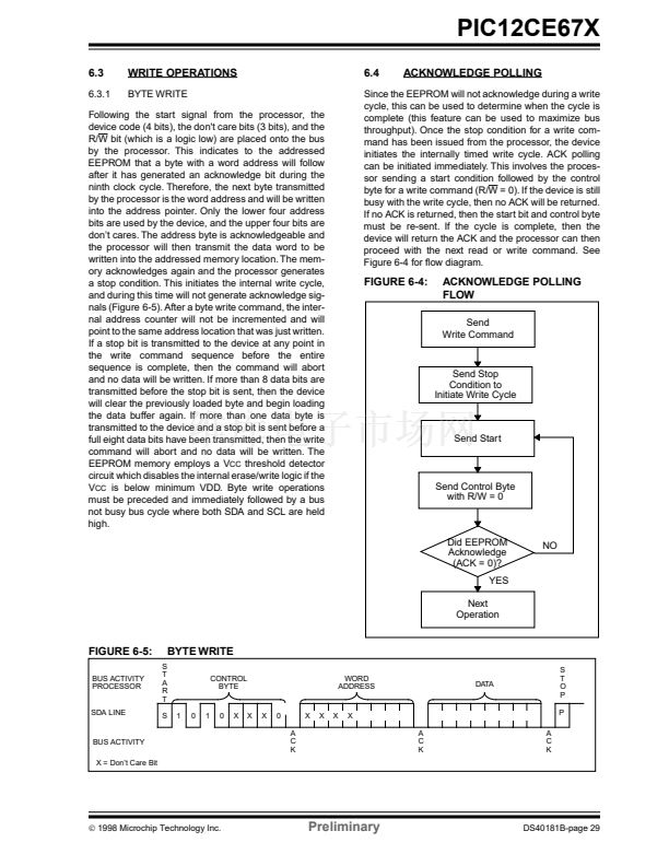
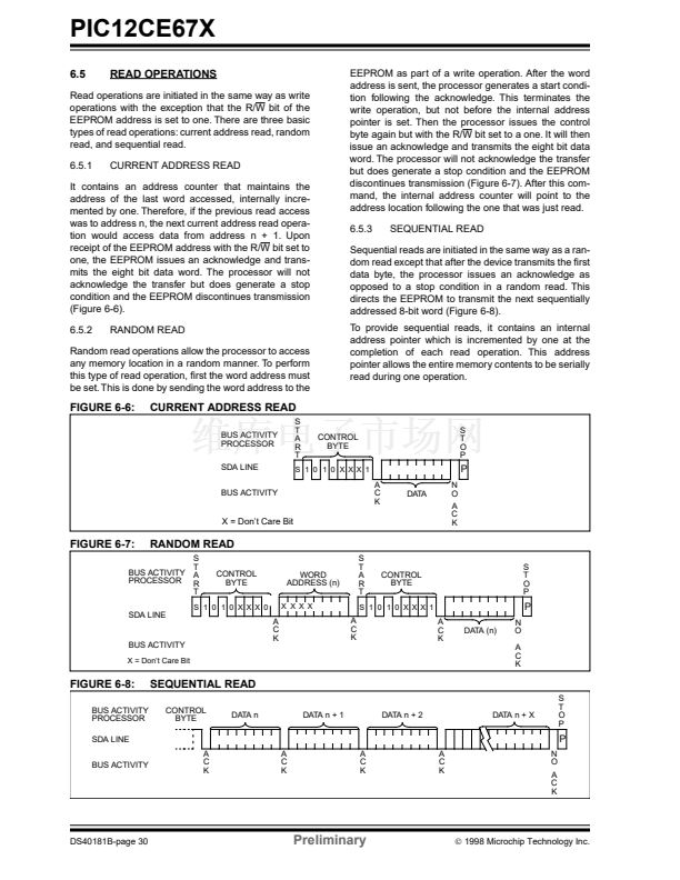
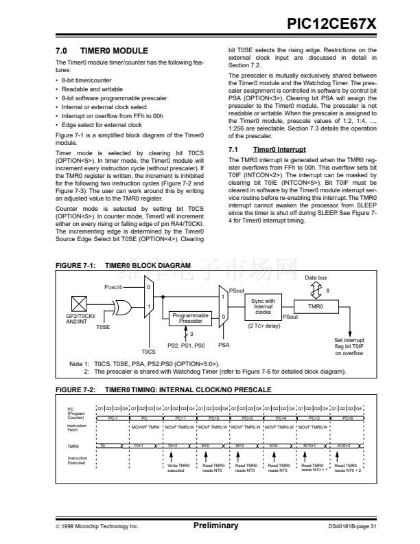
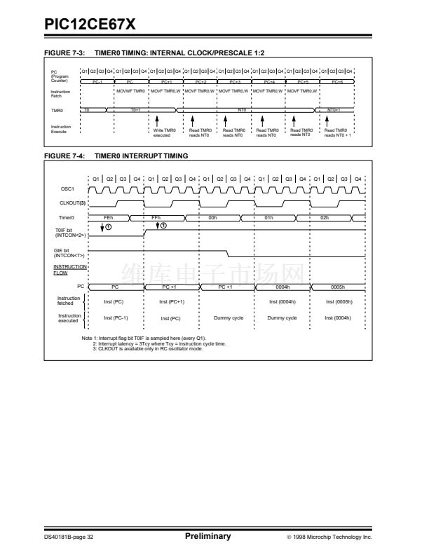
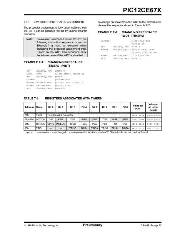
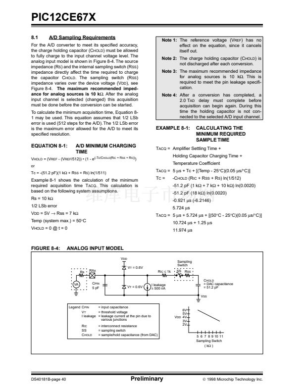
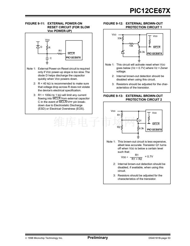
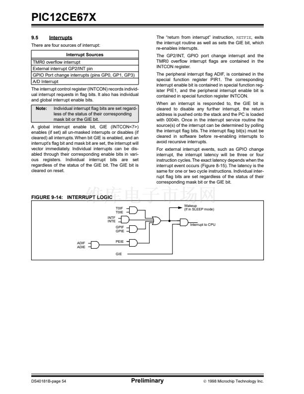
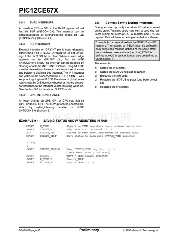
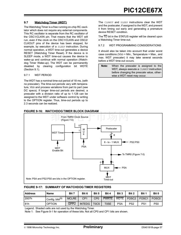
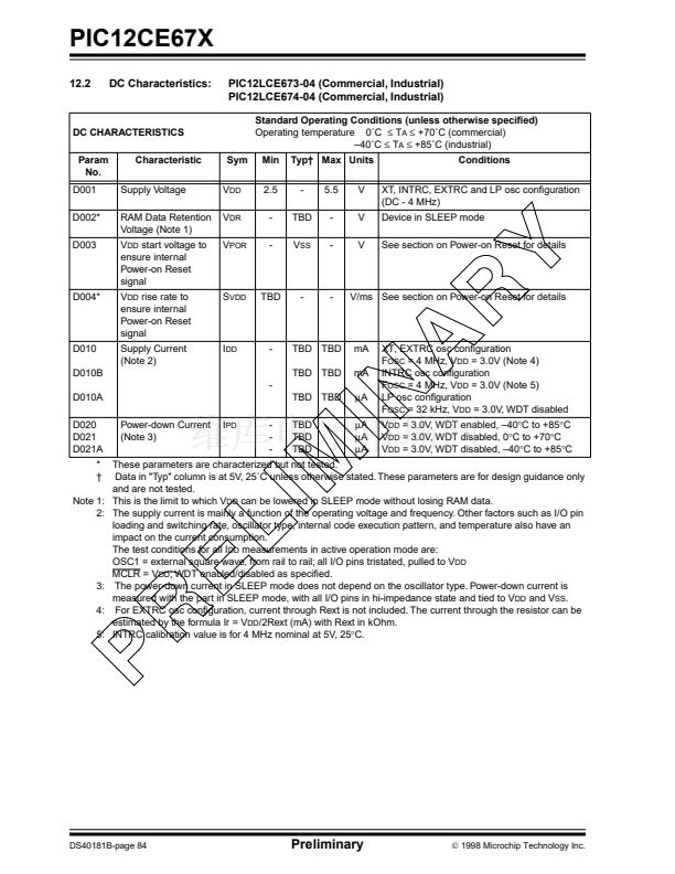
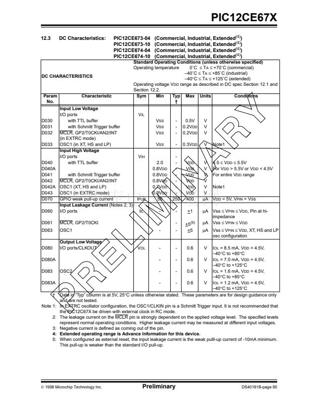
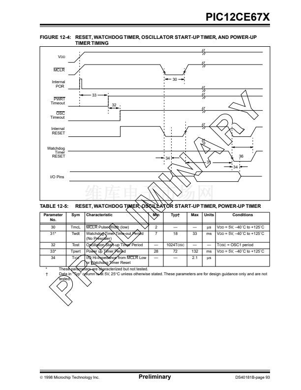
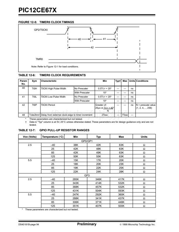
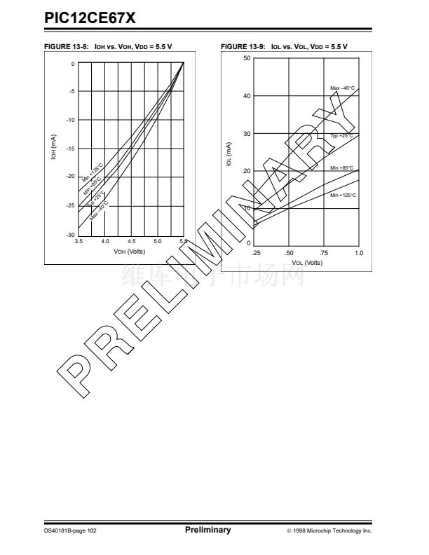
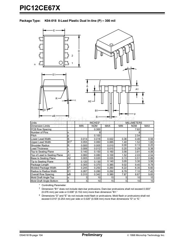
PIC12CE67X
8.5
A/D Operation During Sleep
8.7
Effects of a RESET
The A/D module can operate during SLEEP mode. This
requires that the A/D clock source be set to RC
(ADCS1:ADCS0 =
11).
When the RC clock source is
selected, the A/D module waits one instruction cycle
before starting the conversion. This allows the
SLEEP
instruction to be executed, which eliminates all digital
switching noise from the conversion. When the conver-
sion is completed the GO/DONE bit will be cleared, and
the result loaded into the ADRES register. If the A/D
interrupt is enabled, the device will wake-up from
SLEEP. If the A/D interrupt is not enabled, the A/D mod-
ule will then be turned off, although the ADON bit will
remain set.
When the A/D clock source is another clock option (not
RC), a
SLEEP
instruction will cause the present conver-
sion to be aborted and the A/D module to be turned off,
though the ADON bit will remain set.
Turning off the A/D places the A/D module in its lowest
current consumption state.
Note:
For the A/D module to operate in SLEEP,
the A/D clock source must be set to RC
(ADCS1:ADCS0 =
11).
To perform an A/D
conversion in SLEEP, the GO/DONE bit
must be set, followed by the
SLEEP
instruc-
tion.
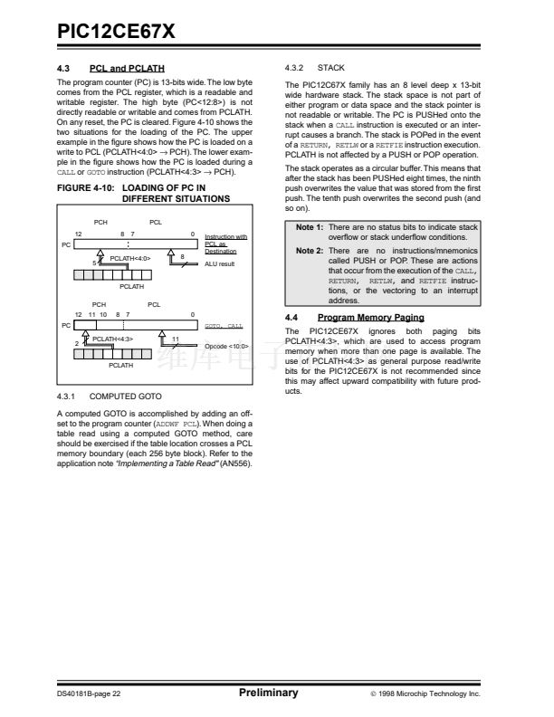
A device reset forces all registers to their reset state.
This forces the A/D module to be turned off, and any
conversion is aborted. The value that is in the ADRES
register is not modi铿乪d for a Reset. The ADRES regis-
ter will contain unknown data after a Power-on Reset.
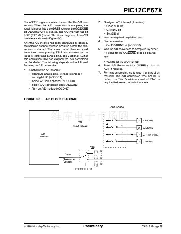
8.8
Connection Considerations
If the input voltage exceeds the rail values (V
SS
or V
DD
)
by greater than 0.2V, then the accuracy of the conver-
sion is out of speci铿乧ation.
Note:
For the PIC12CE67X, care must be taken
when using the GP4 pin in A/D conver-
sions due to its proximity to the OSC1 pin.
An external RC 铿乴ter is sometimes added for anti-alias-
ing of the input signal. The R component should be
selected to ensure that the total source impedance is
kept under the 10 k鈩?recommended speci铿乧ation. Any
external components connected (via hi-impedance) to
an analog input pin (capacitor, zener diode, etc.) should
have very little leakage current at the pin.
8.9
Transfer Function
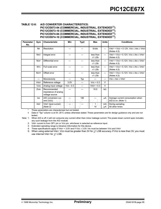
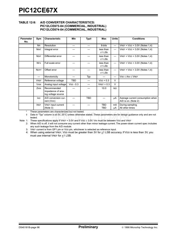
8.6
A/D Accuracy/Error
The ideal transfer function of the A/D converter is as fol-
lows: the first transition occurs when the analog input
voltage (V
AIN
) is 1 LSb (or Analog V
REF
/ 256)
(Figure 8-5).
Digital code output
The overall accuracy of the A/D is less than
卤
1 LSb for
V
DD
= 5V
卤
10% and the analog V
REF
= V
DD
. This over-
all accuracy includes offset error, full scale error, and
integral error. The A/D converter is guaranteed to be
monotonic. The resolution and accuracy may be less
when either the analog reference (V
DD
) is less than
5.0V or when the analog reference (V
REF
) is less than
V
DD
.
The maximum pin leakage current is
卤
5
碌A.
In systems where the device frequency is low, use of
the A/D RC clock is preferred. At moderate to high fre-
quencies, T
AD
should be derived from the device oscil-
lator. T
AD
must not violate the minimum and should be
鈮?/div>
8
碌s
for preferred operation. This is because T
AD
,
when derived from T
OSC
, is kept away from on-chip
phase clock transitions. This reduces, to a large extent,
the effects of digital switching noise. This is not possible
with the RC derived clock. The loss of accuracy due to
digital switching noise can be signi铿乧ant if many I/O
pins are active.
In systems where the device will enter SLEEP mode
after the start of the A/D conversion, the RC clock
source selection is required. In this mode, the digital
noise from the modules in SLEEP are stopped. This
method gives high accuracy.
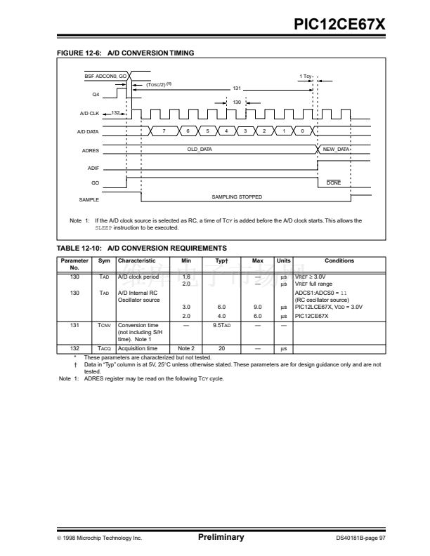
FIGURE 8-5:
A/D TRANSFER FUNCTION
FFh
FEh
04h
03h
02h
01h
00h
256 LSb
(full scale)
255 LSb
0.5 LSb
1 LSb
2 LSb
3 LSb
4 LSb
Analog input voltage
漏
1998 Microchip Technology Inc.
Preliminary
DS40181B-page 43


 1
1
 2
2
 3
3
 4
4
 5
5
 6
6
 7
7
 8
8
 9
9
 10
10
 11
11
 12
12
 13
13
 14
14
 15
15
 16
16
 17
17
 18
18
 19
19
 20
20
 21
21
 22
22
 23
23
 24
24
 25
25
 26
26
 27
27
 28
28
 29
29
 30
30
 31
31
 32
32
 33
33
 34
34
 35
35
 36
36
 37
37
 38
38
 39
39
 40
40
 41
41
 42
42
 43
43
 44
44
 45
45
 46
46
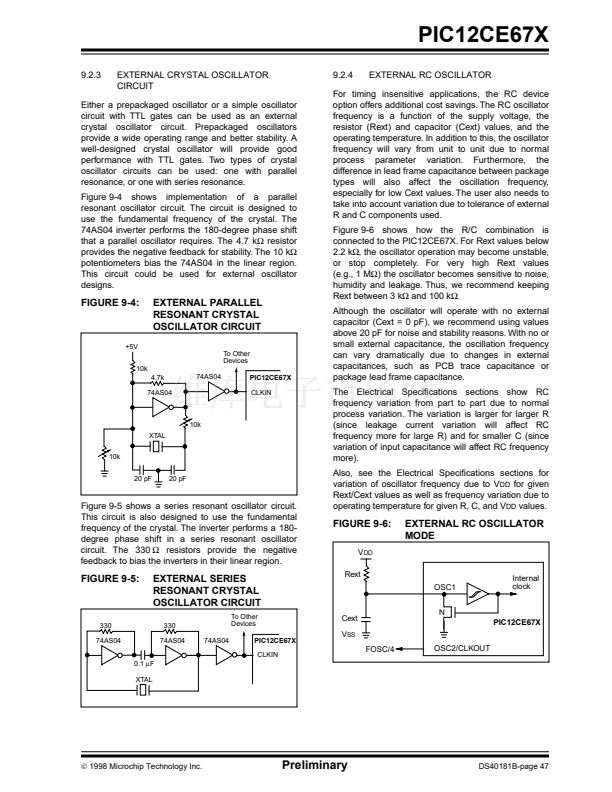 47
47
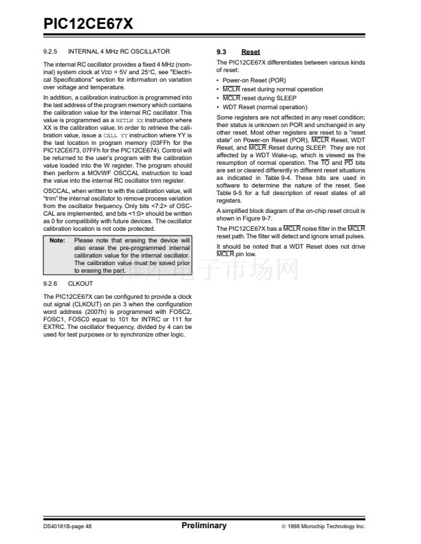 48
48
 49
49
 50
50
 51
51
 52
52
 53
53
 54
54
 55
55
 56
56
 57
57
 58
58
 59
59
 60
60
 61
61
 62
62
 63
63
 64
64
 65
65
 66
66
 67
67
 68
68
 69
69
 70
70
 71
71
 72
72
 73
73
 74
74
 75
75
 76
76
 77
77
 78
78
 79
79
 80
80
 81
81
 82
82
 83
83
 84
84
 85
85
 86
86
 87
87
 88
88
 89
89
 90
90
 91
91
 92
92
 93
93
 94
94
 95
95
 96
96
 97
97
 98
98
 99
99
 100
100
 101
101
 102
102
 103
103
 104
104
 105
105
 106
106
 107
107
 108
108
 109
109
 110
110
 111
111
 112
112
 113
113
 114
114
 115
115
 116
116
