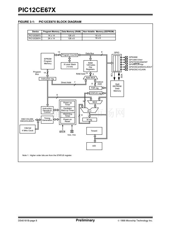
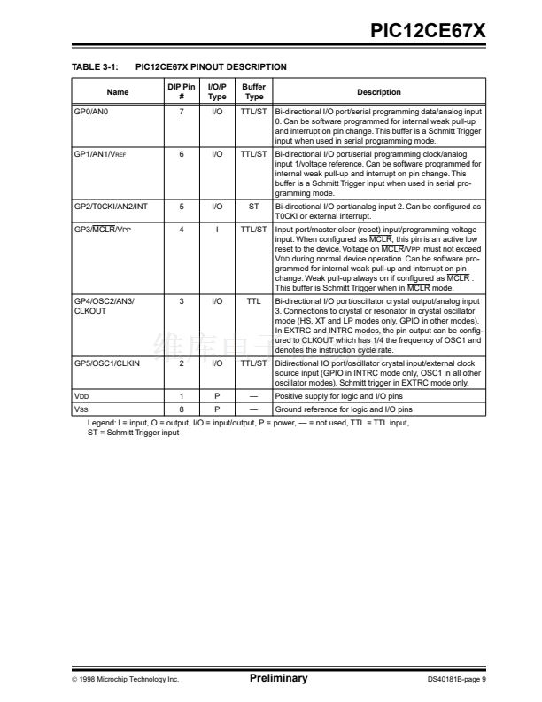
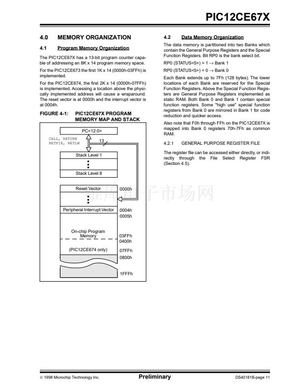
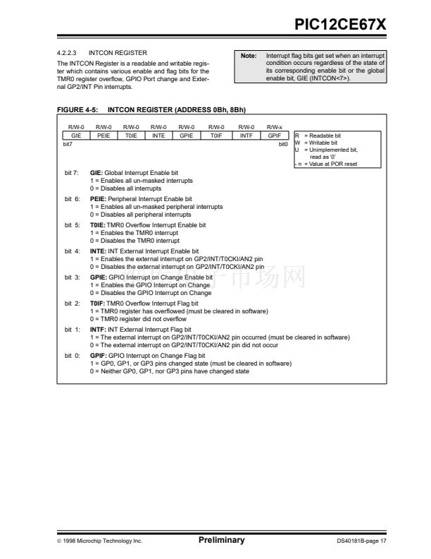
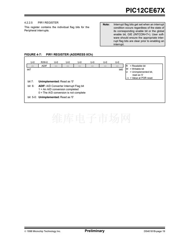
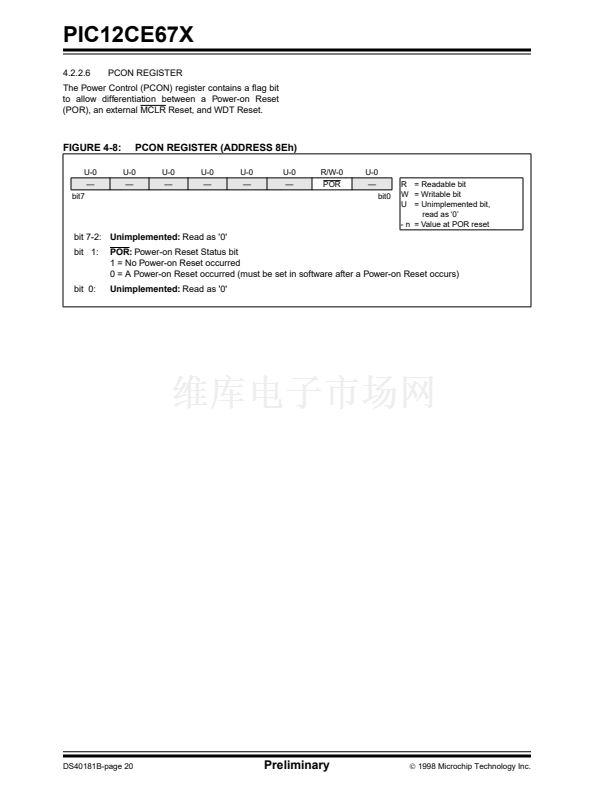
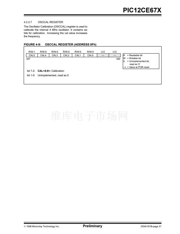
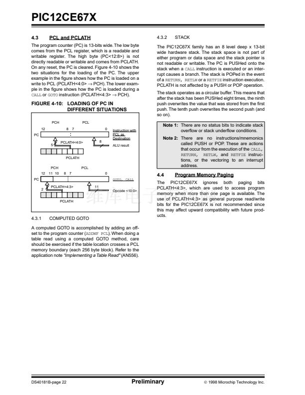
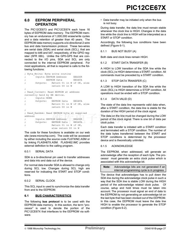
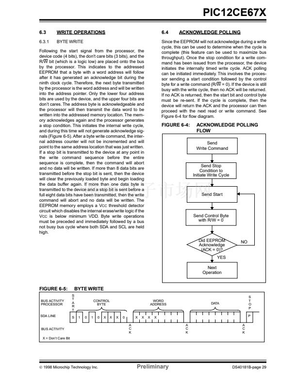
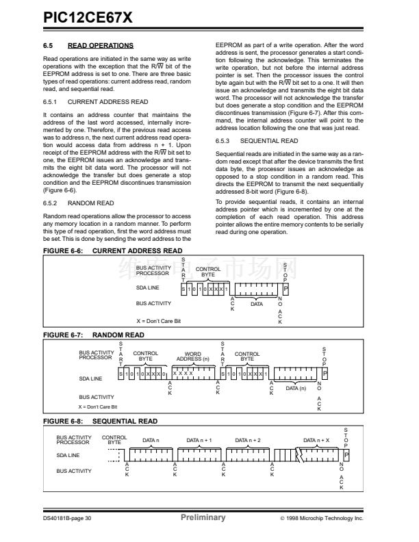
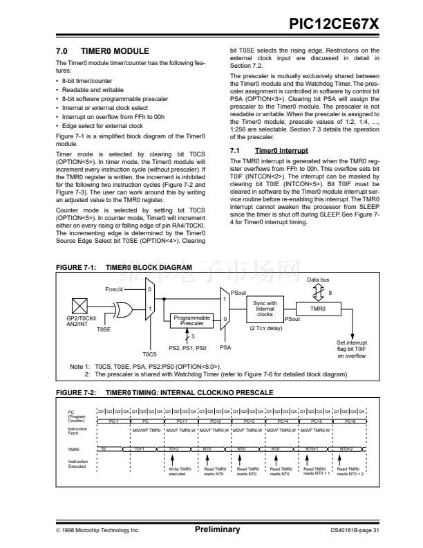
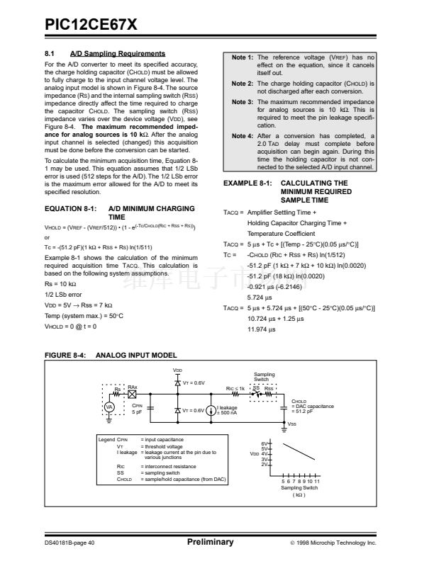
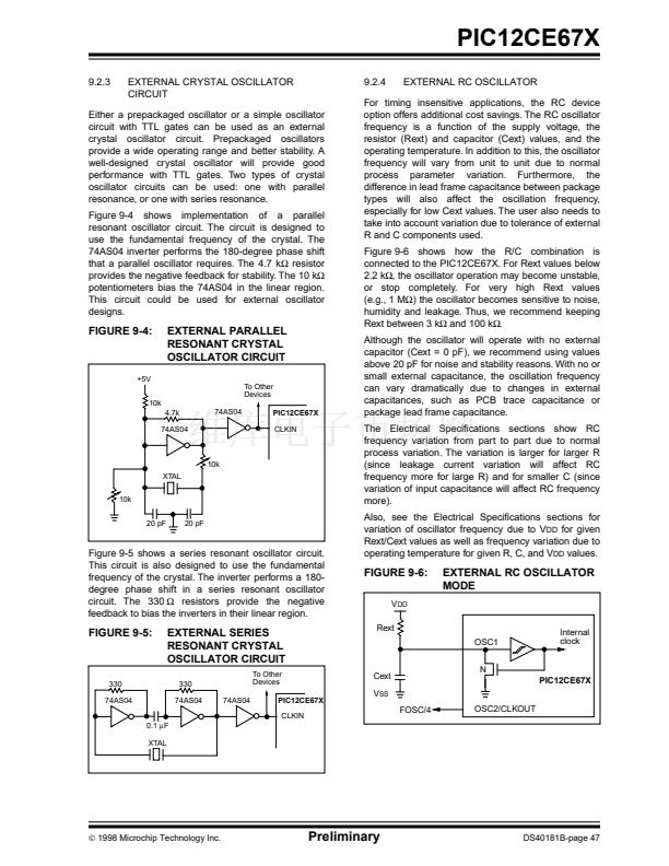
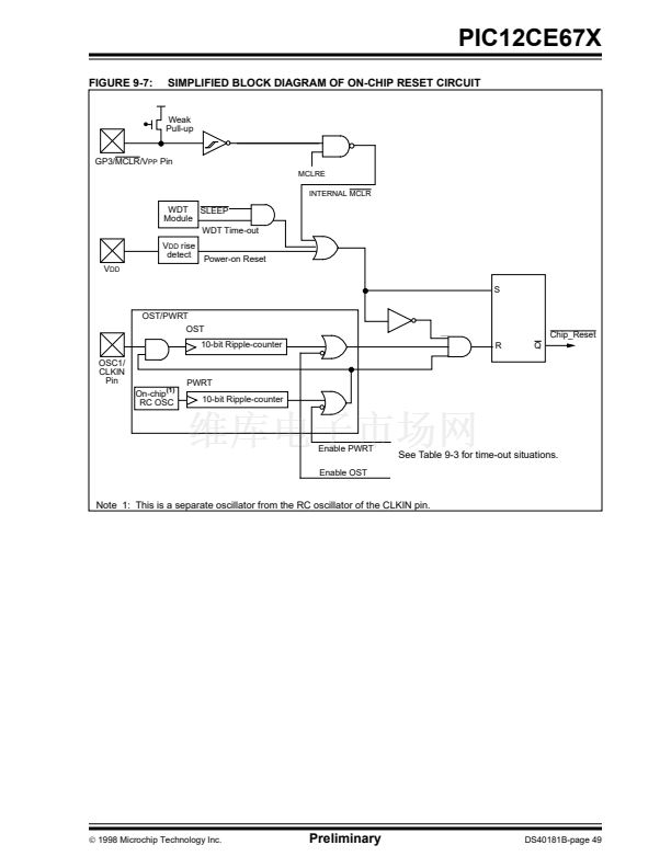
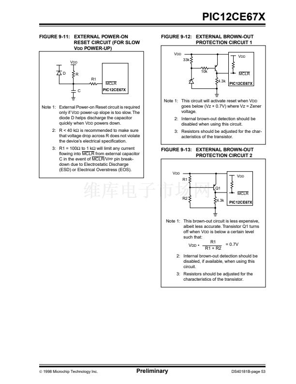
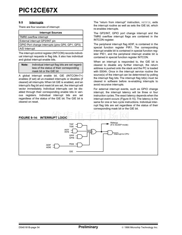
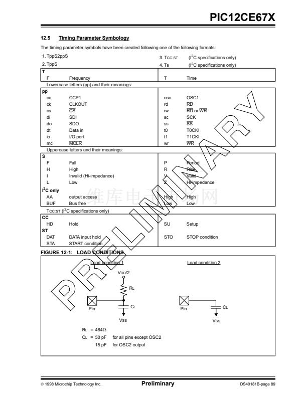
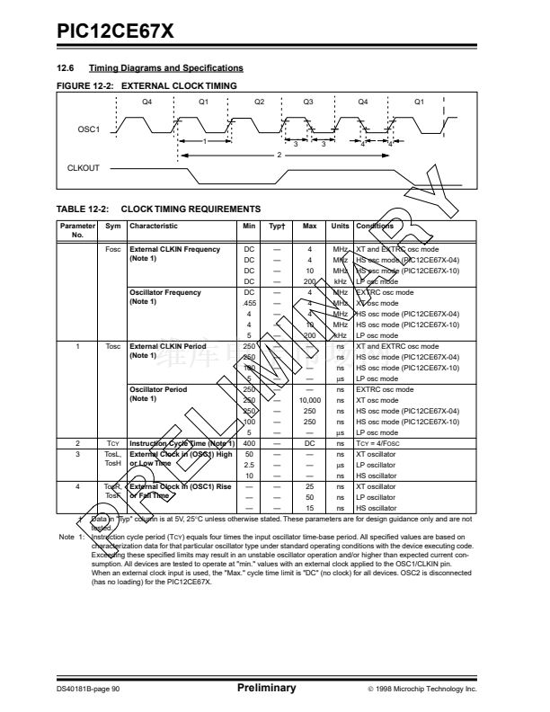
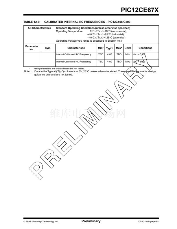
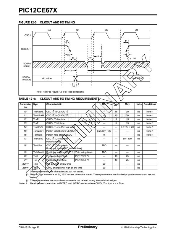
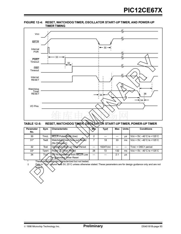
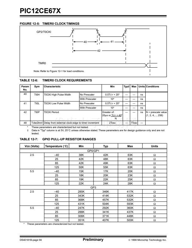
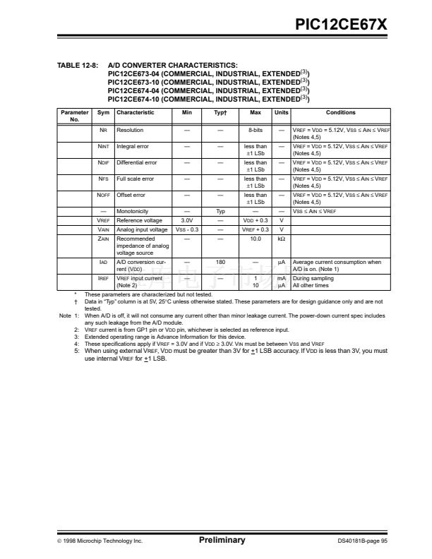
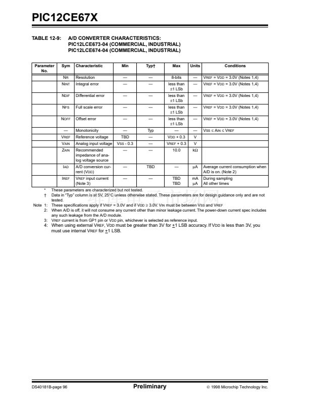
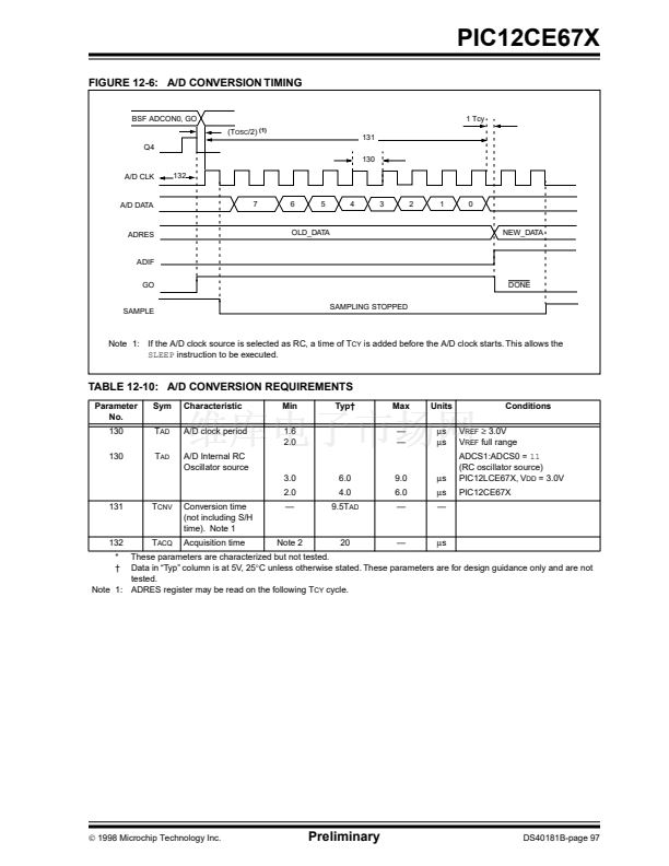
PIC12CE67X
9.7
Watchdog Timer (WDT)
The Watchdog Timer is a free running on-chip RC oscil-
lator which does not require any external components.
This RC oscillator is separate from the RC oscillator of
the OSC1/CLKIN pin. That means that the WDT will
run, even if the clock on the OSC1/CLKIN and OSC2/
CLKOUT pins of the device has been stopped, for
example, by execution of a
SLEEP
instruction. During
normal operation, a WDT time-out generates a device
RESET (Watchdog Timer Reset). If the device is in
SLEEP mode, a WDT time-out causes the device to
wake-up and continue with normal operation (Watch-
dog Timer Wake-up). The WDT can be permanently
disabled by clearing con铿乬uration bit WDTE
(Section 9.1).
9.7.1
WDT PERIOD
The
CLRWDT
and
SLEEP
instructions clear the WDT
and the postscaler, if assigned to the WDT, and prevent
it from timing out early and generating a premature
device RESET condition.
The TO bit in the STATUS register will be cleared upon
a Watchdog Timer time-out.
9.7.2
WDT PROGRAMMING CONSIDERATIONS
It should also be taken into account that under worst
case conditions (V
DD
= Min., Temperature = Max., and
max. WDT prescaler) it may take several seconds
before a WDT time-out occurs.
Note:
When the prescaler is assigned to the
WDT, always execute a
CLRWDT
instruction
before changing the prescale value, other-
wise a WDT reset may occur.
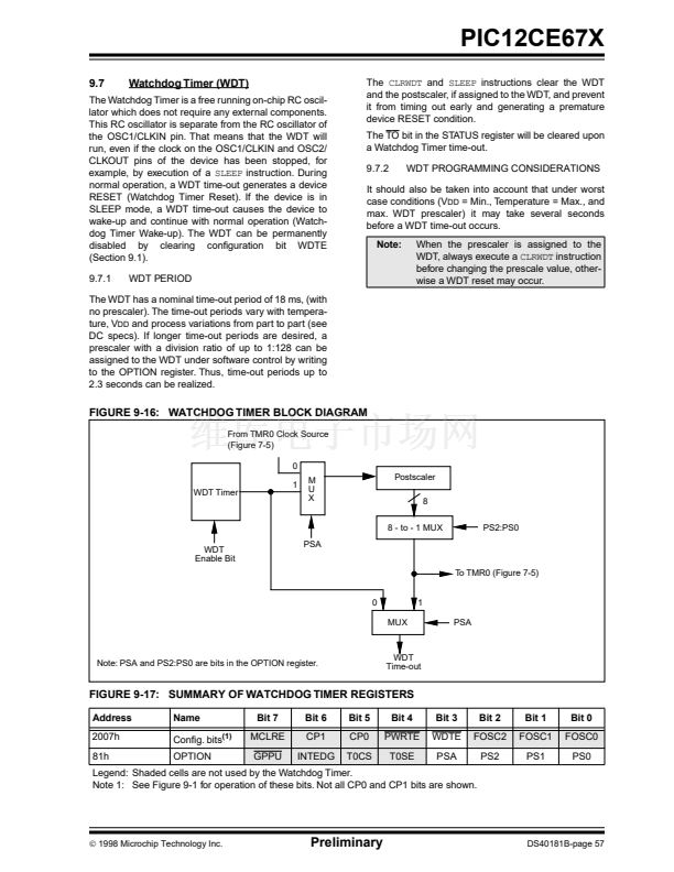
The WDT has a nominal time-out period of 18 ms, (with
no prescaler). The time-out periods vary with tempera-
ture, V
DD
and process variations from part to part (see
DC specs). If longer time-out periods are desired, a
prescaler with a division ratio of up to 1:128 can be
assigned to the WDT under software control by writing
to the OPTION register. Thus, time-out periods up to
2.3 seconds can be realized.
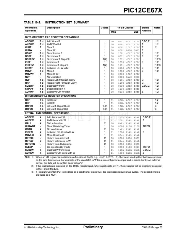
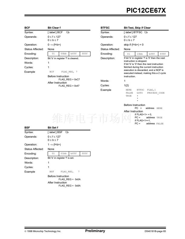
FIGURE 9-16: WATCHDOG TIMER BLOCK DIAGRAM
From TMR0 Clock Source
(Figure 7-5)
0
WDT Timer
1
M
U
X
Postscaler
8
8 - to - 1 MUX
WDT
Enable Bit
PSA
To TMR0 (Figure 7-5)
0
MUX
1
PSA
PS2:PS0
Note: PSA and PS2:PS0 are bits in the OPTION register.
WDT
Time-out
FIGURE 9-17: SUMMARY OF WATCHDOG TIMER REGISTERS
Address
2007h
81h
Name
Con铿乬. bits
(1)
OPTION
Bit 7
MCLRE
GPPU
Bit 6
CP1
INTEDG
Bit 5
CP0
T0CS
Bit 4
PWRTE
T0SE
Bit 3
WDTE
PSA
Bit 2
FOSC2
PS2
Bit 1
FOSC1
PS1
Bit 0
FOSC0
PS0
Legend: Shaded cells are not used by the Watchdog Timer.
Note 1: See Figure 9-1 for operation of these bits. Not all CP0 and CP1 bits are shown.
漏
1998 Microchip Technology Inc.
Preliminary
DS40181B-page 57


 1
1
 2
2
 3
3
 4
4
 5
5
 6
6
 7
7
 8
8
 9
9
 10
10
 11
11
 12
12
 13
13
 14
14
 15
15
 16
16
 17
17
 18
18
 19
19
 20
20
 21
21
 22
22
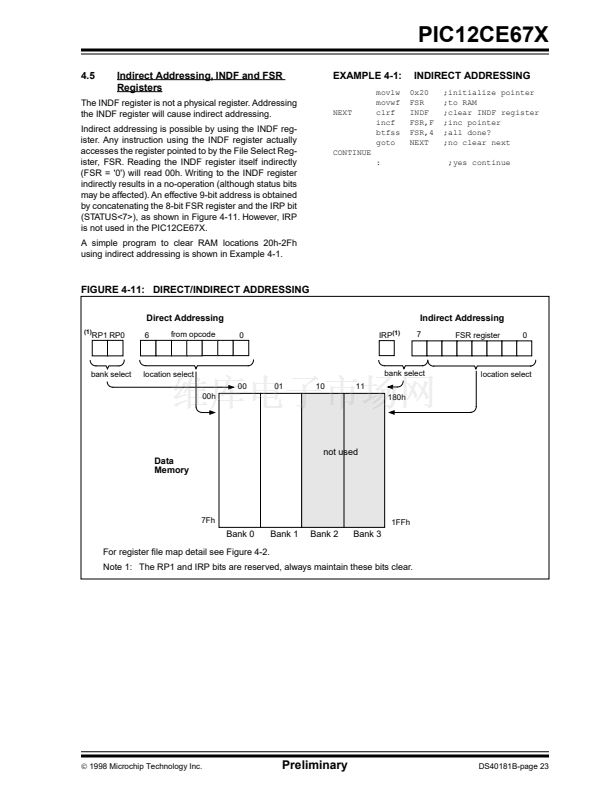 23
23
 24
24
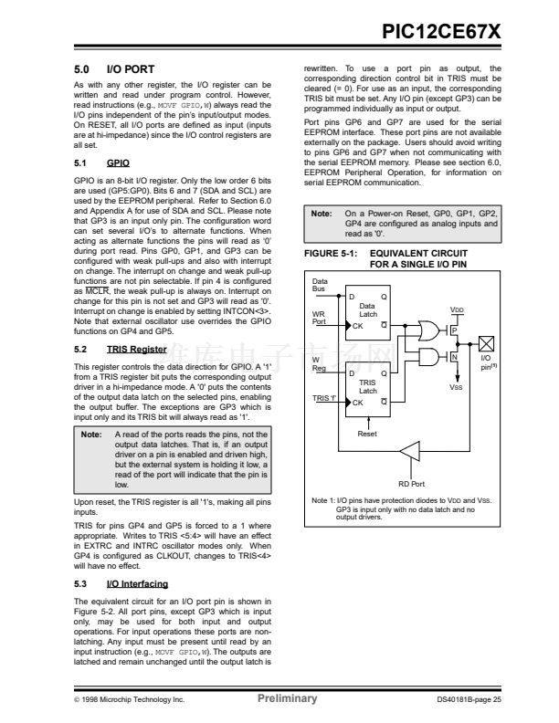 25
25
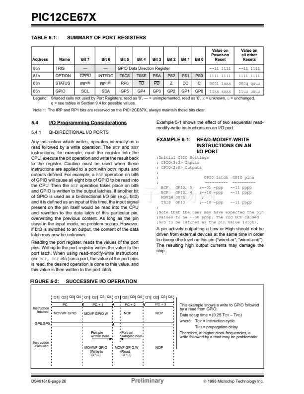 26
26
 27
27
 28
28
 29
29
 30
30
 31
31
 32
32
 33
33
 34
34
 35
35
 36
36
 37
37
 38
38
 39
39
 40
40
 41
41
 42
42
 43
43
 44
44
 45
45
 46
46
 47
47
 48
48
 49
49
 50
50
 51
51
 52
52
 53
53
 54
54
 55
55
 56
56
 57
57
 58
58
 59
59
 60
60
 61
61
 62
62
 63
63
 64
64
 65
65
 66
66
 67
67
 68
68
 69
69
 70
70
 71
71
 72
72
 73
73
 74
74
 75
75
 76
76
 77
77
 78
78
 79
79
 80
80
 81
81
 82
82
 83
83
 84
84
 85
85
 86
86
 87
87
 88
88
 89
89
 90
90
 91
91
 92
92
 93
93
 94
94
 95
95
 96
96
 97
97
 98
98
 99
99
 100
100
 101
101
 102
102
 103
103
 104
104
 105
105
 106
106
 107
107
 108
108
 109
109
 110
110
 111
111
 112
112
 113
113
 114
114
 115
115
 116
116
