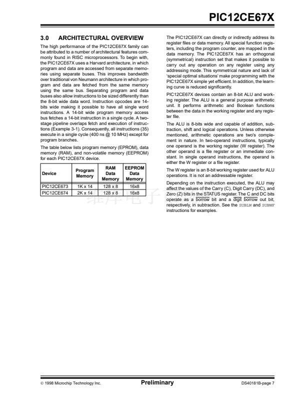
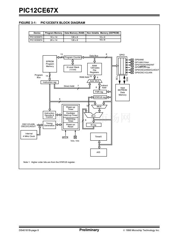
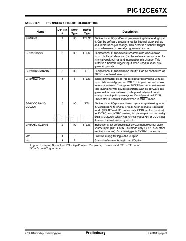
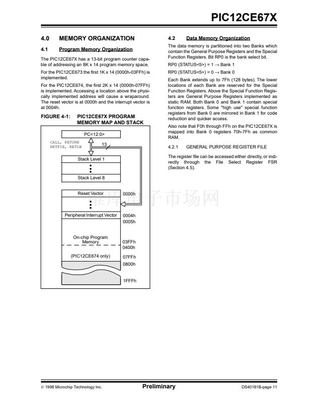
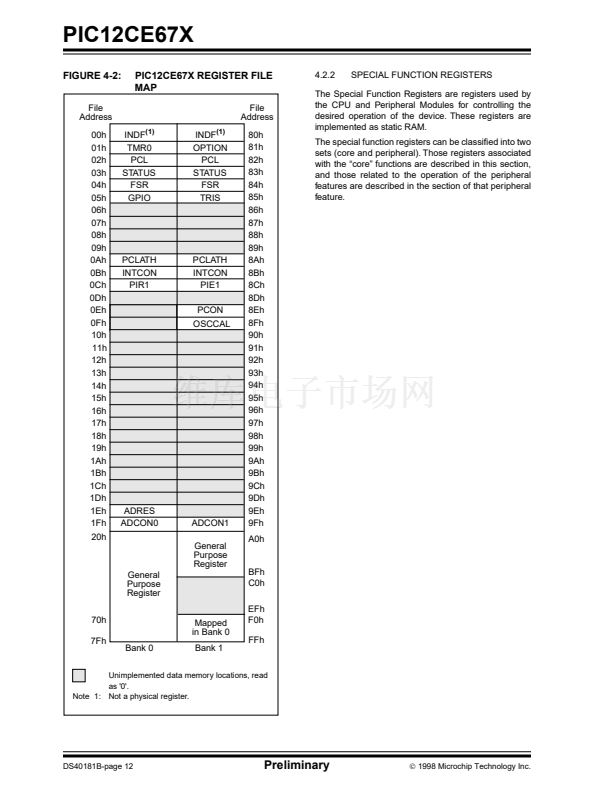
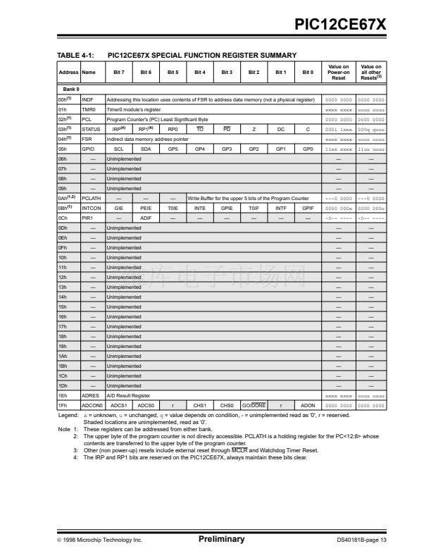
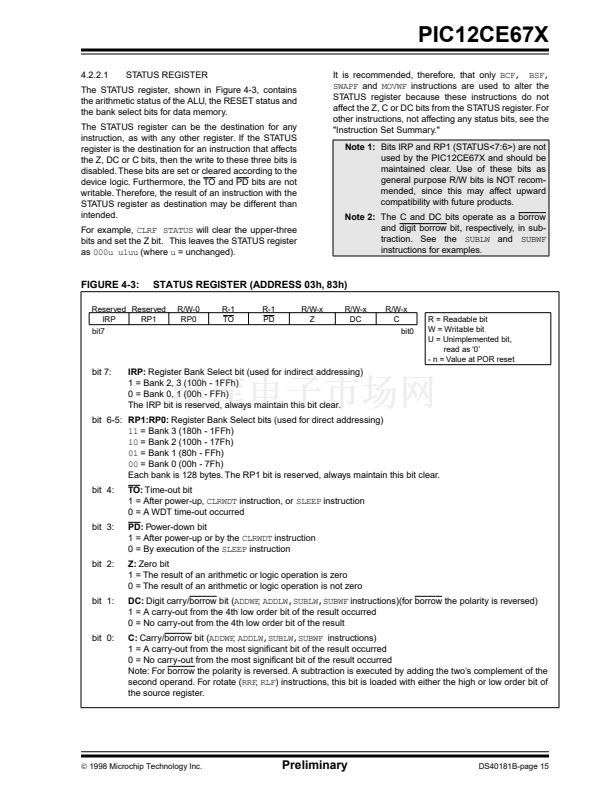
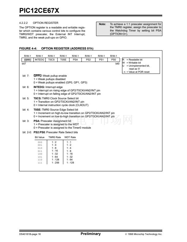
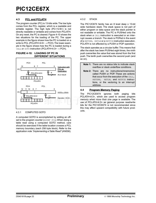
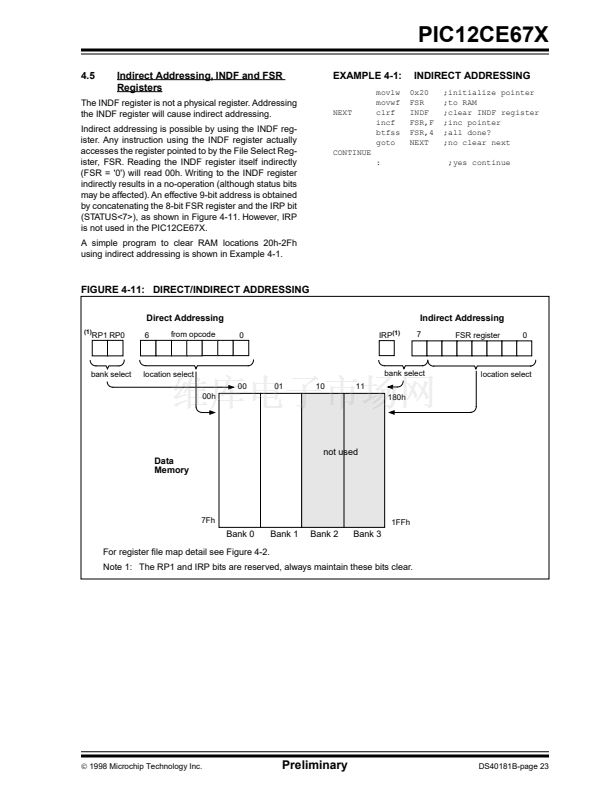
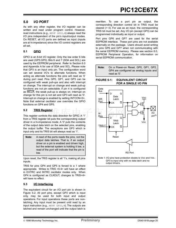
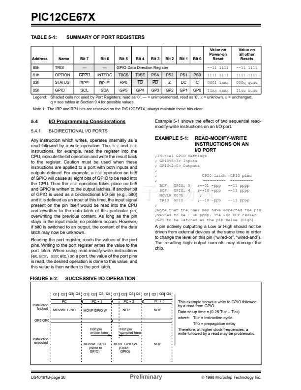
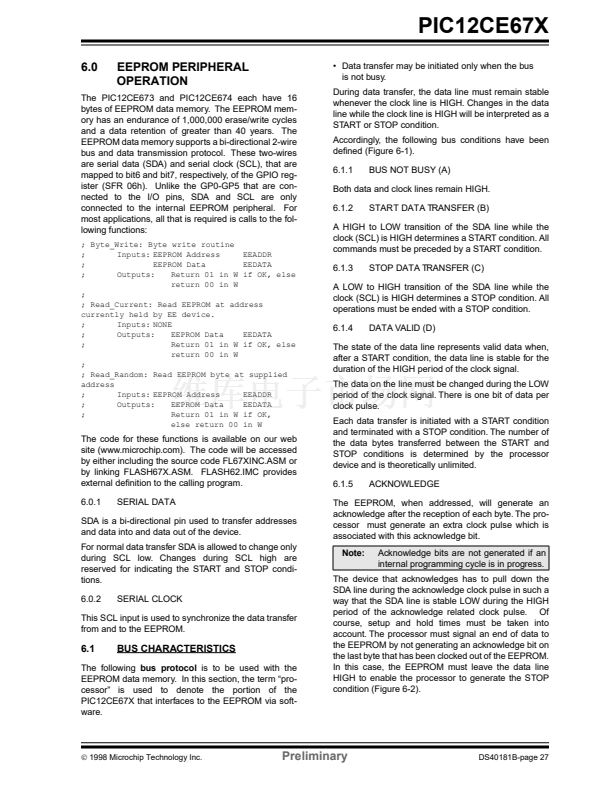
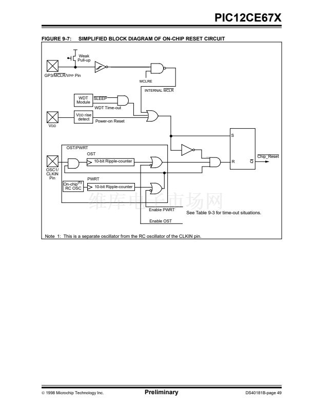
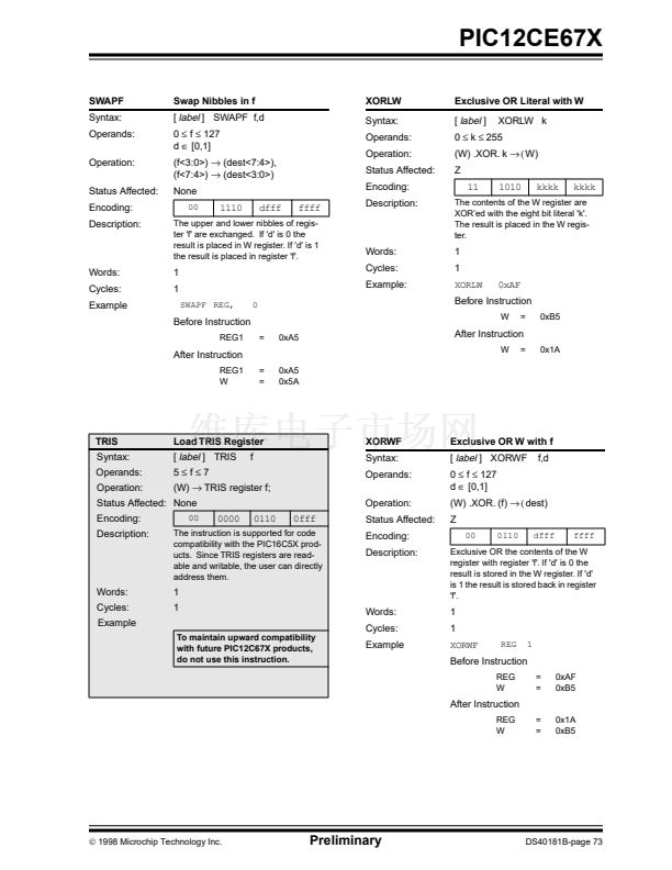
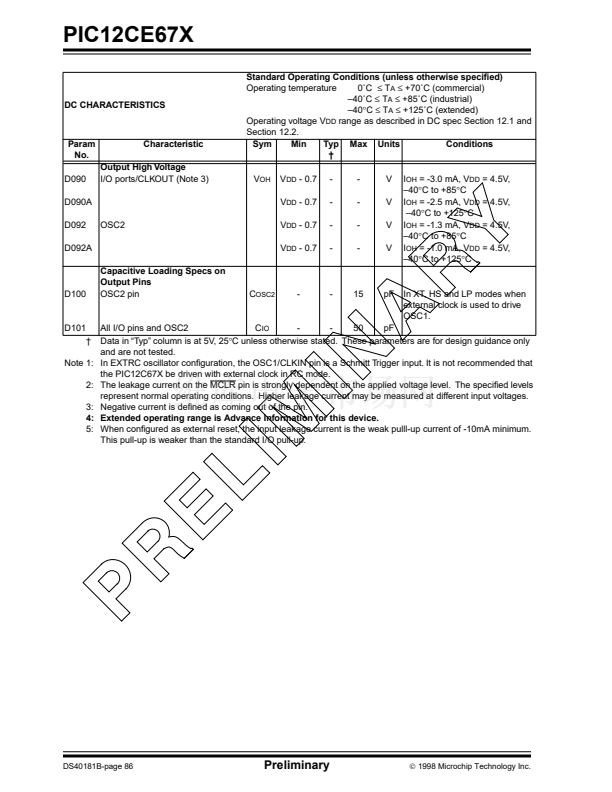
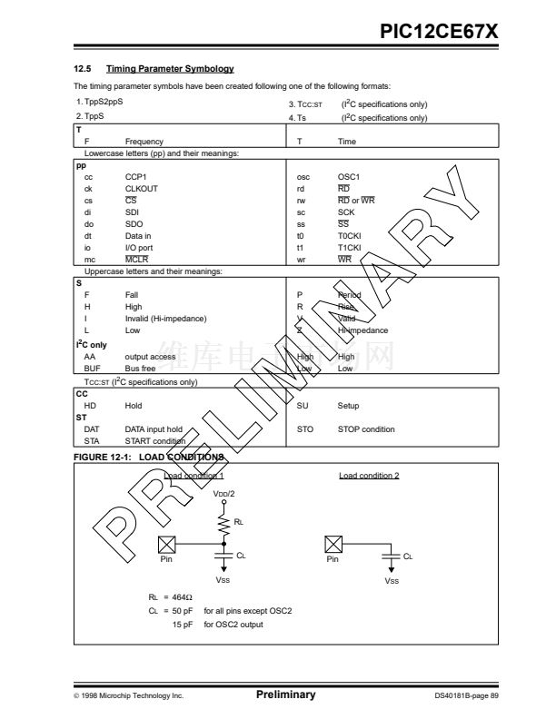
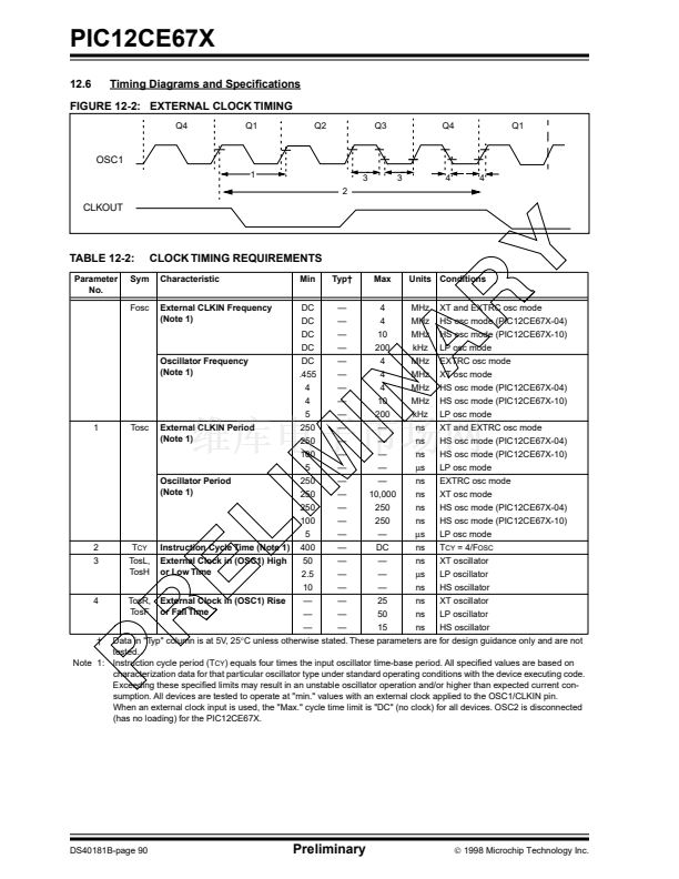
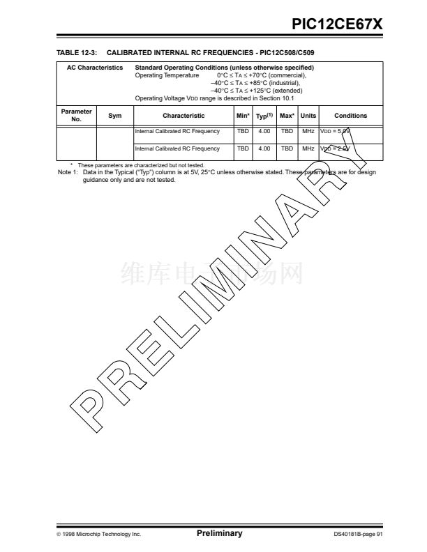
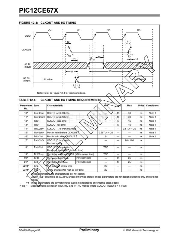
鈥?/div>
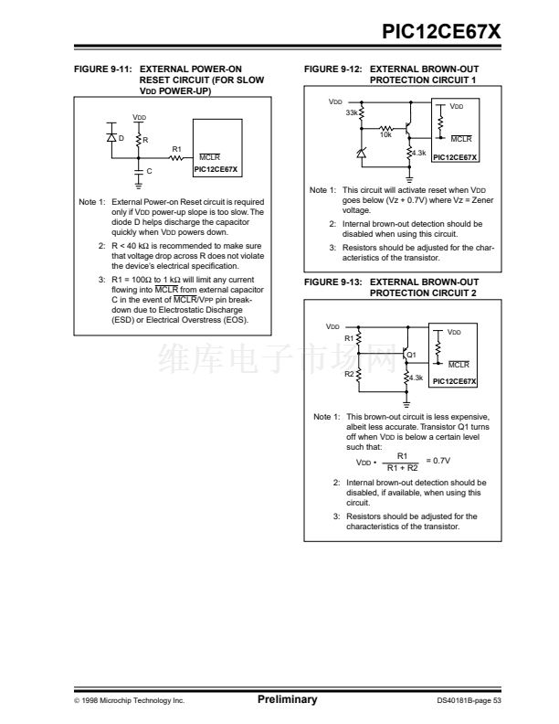
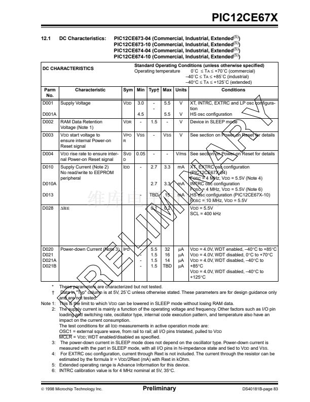
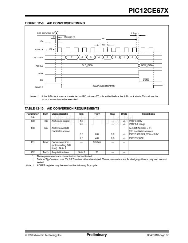
Note 1:
2:
3:
4:
I
OH
= TBD, V
DD
= 4.5V,
鈥?0掳C to +85掳C
V
DD
- 0.7 -
-
V I
OH
= TBD, V
DD
= 4.5V,
鈥?0掳C to +125掳C
OSC2
V
DD
- 0.7 -
-
V I
OH
= TBD, V
DD
= 4.5V,
鈥?0掳C to +85掳C
V
DD
- 0.7 -
-
V I
OH
= TBD, V
DD
= 4.5V,
鈥?0掳C to +125掳C
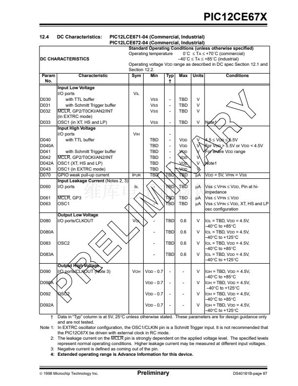
Data in 鈥淭yp鈥?column is at 5V, 25掳C unless otherwise stated. These parameters are for design guidance only
and are not tested.
In EXTRC oscillator con铿乬uration, the OSC1/CLKIN pin is a Schmitt Trigger input. It is not recommended that
the PIC12C67X be driven with external clock in RC mode.
The leakage current on the MCLR pin is strongly dependent on the applied voltage level. The speci铿乪d levels
represent normal operating conditions. Higher leakage current may be measured at different input voltages.
Negative current is de铿乶ed as coming out of the pin.
Extended operating range is Advance Information for this device.
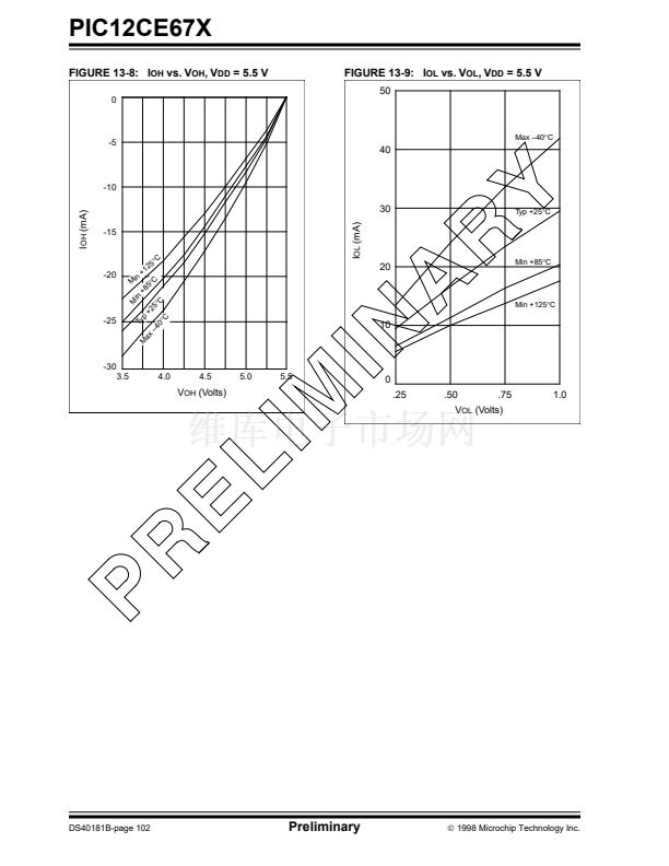
Output High Voltage
I/O ports/CLKOUT (Note 3)
V
OH
V
DD
- 0.7
-
-
V
漏
1998 Microchip Technology Inc.
Preliminary
DS40181B-page 87


 1
1
 2
2
 3
3
 4
4
 5
5
 6
6
 7
7
 8
8
 9
9
 10
10
 11
11
 12
12
 13
13
 14
14
 15
15
 16
16
 17
17
 18
18
 19
19
 20
20
 21
21
 22
22
 23
23
 24
24
 25
25
 26
26
 27
27
 28
28
 29
29
 30
30
 31
31
 32
32
 33
33
 34
34
 35
35
 36
36
 37
37
 38
38
 39
39
 40
40
 41
41
 42
42
 43
43
 44
44
 45
45
 46
46
 47
47
 48
48
 49
49
 50
50
 51
51
 52
52
 53
53
 54
54
 55
55
 56
56
 57
57
 58
58
 59
59
 60
60
 61
61
 62
62
 63
63
 64
64
 65
65
 66
66
 67
67
 68
68
 69
69
 70
70
 71
71
 72
72
 73
73
 74
74
 75
75
 76
76
 77
77
 78
78
 79
79
 80
80
 81
81
 82
82
 83
83
 84
84
 85
85
 86
86
 87
87
 88
88
 89
89
 90
90
 91
91
 92
92
 93
93
 94
94
 95
95
 96
96
 97
97
 98
98
 99
99
 100
100
 101
101
 102
102
 103
103
 104
104
 105
105
 106
106
 107
107
 108
108
 109
109
 110
110
 111
111
 112
112
 113
113
 114
114
 115
115
 116
116
