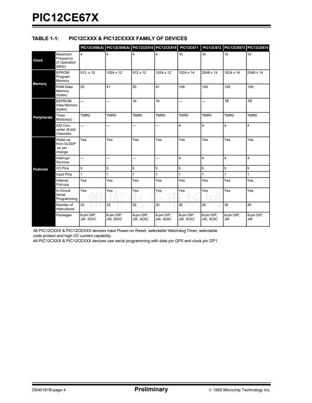
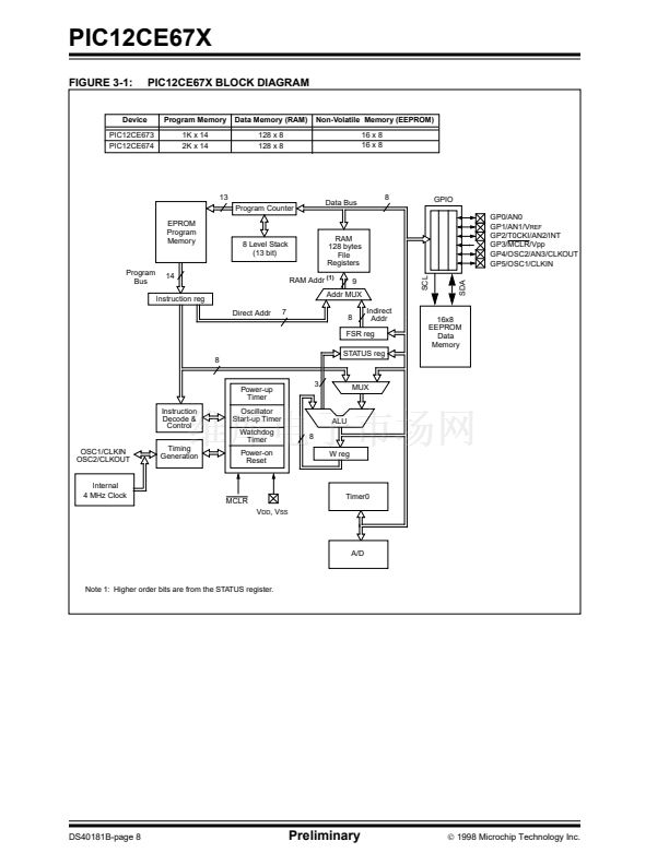
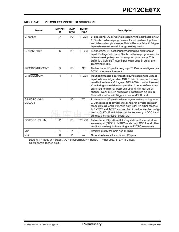
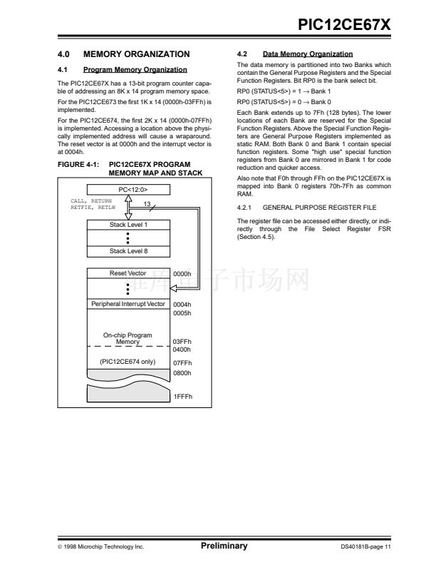
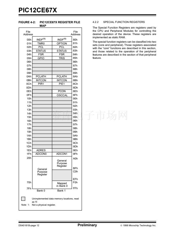
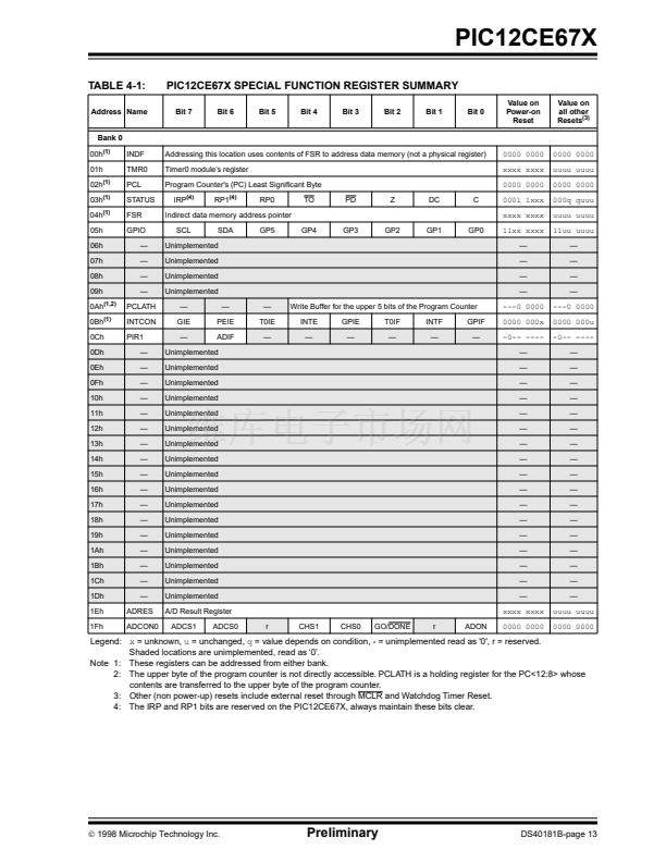
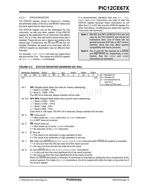
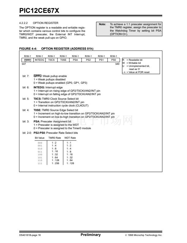
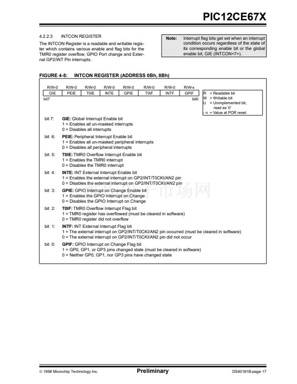
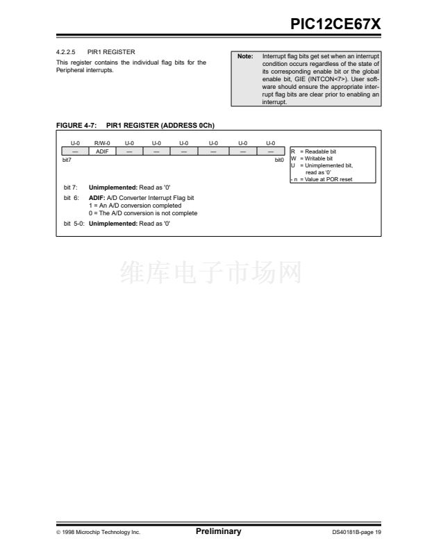
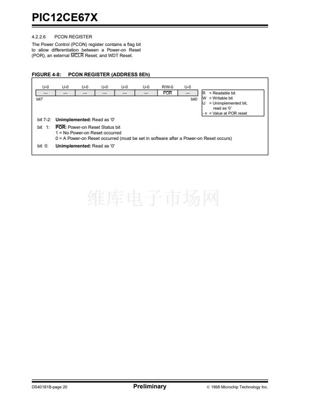
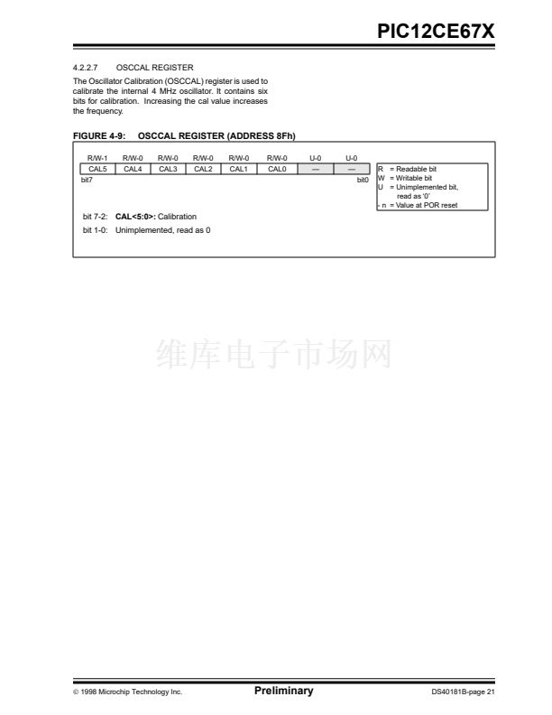
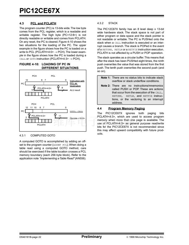
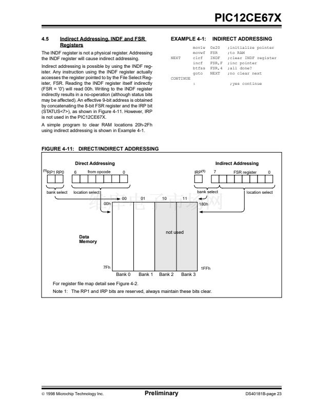
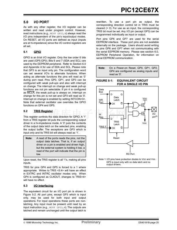
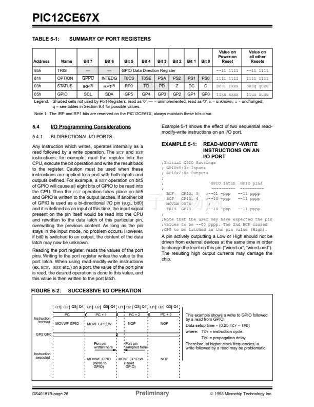
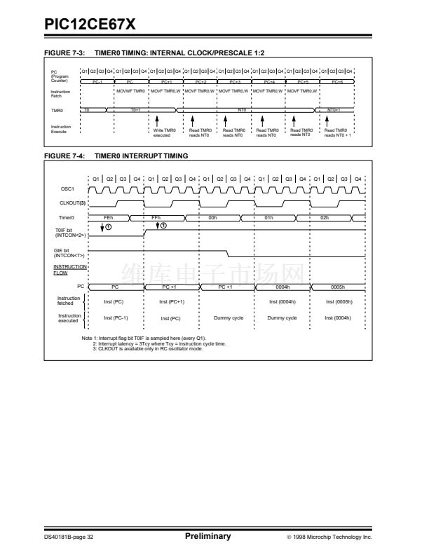
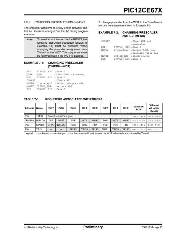
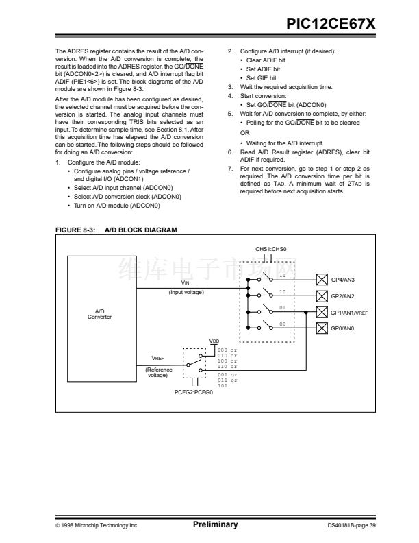
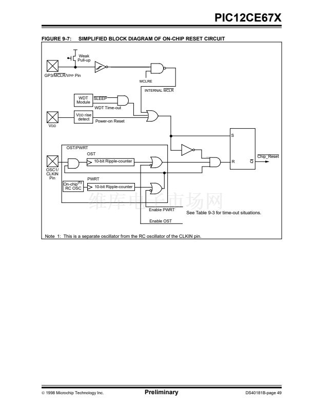
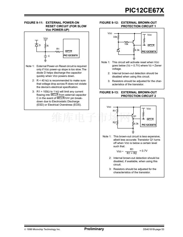
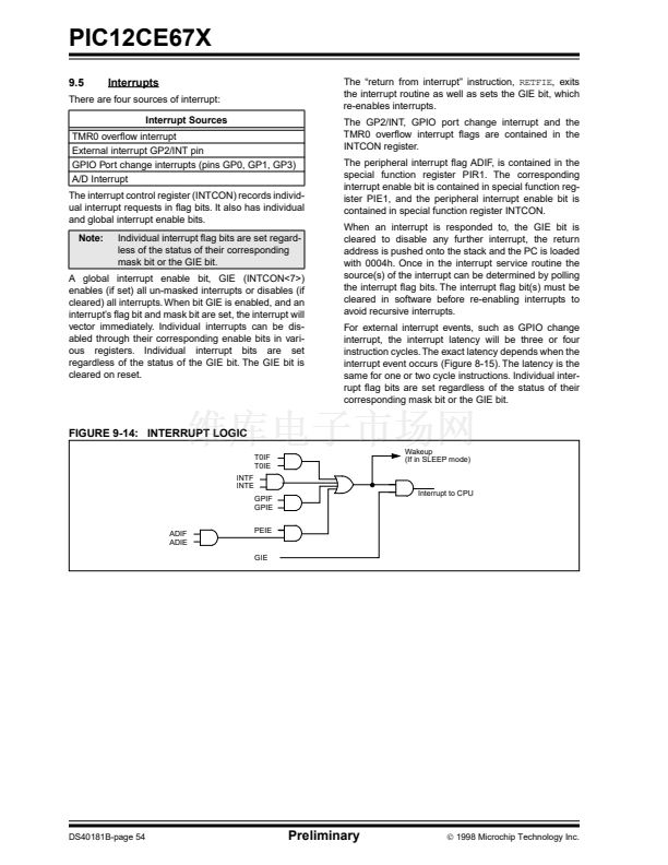
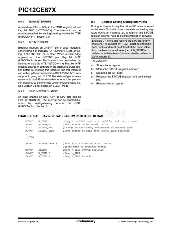
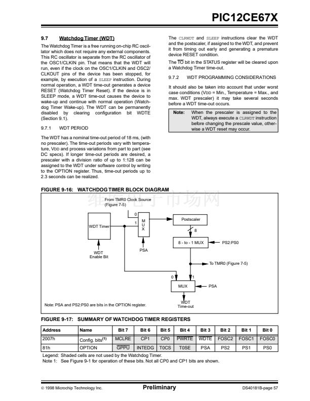
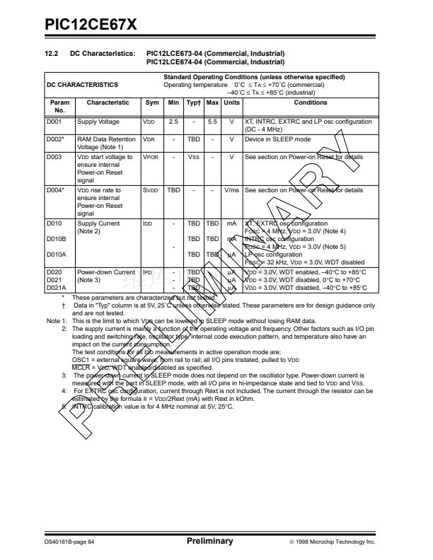
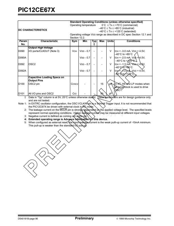
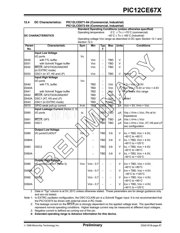
PIC12CE67X
12.5
Timing Parameter Symbology
The timing parameter symbols have been created following one of the following formats:
1. TppS2ppS
2. TppS
T
F
Frequency
Lowercase letters (pp) and their meanings:
pp
cc
CCP1
ck
CLKOUT
cs
CS
di
SDI
do
SDO
dt
Data in
io
I/O port
mc
MCLR
Uppercase letters and their meanings:
S
F
Fall
H
High
I
Invalid (Hi-impedance)
L
Low
I
2
C only
AA
BUF
output access
Bus free
T
Time
3. T
CC
:
ST
4. Ts
(I
2
C speci铿乧ations only)
(I
2
C speci铿乧ations only)
osc
rd
rw
sc
ss
t0
t1
wr
OSC1
RD
RD or WR
SCK
SS
T0CKI
T1CKI
WR
P
R
V
Z
High
Low
Period
Rise
Valid
Hi-impedance
High
Low
T
CC
:
ST
(I
2
C speci铿乧ations only)
CC
HD
Hold
ST
DAT
DATA input hold
STA
START condition
SU
STO
Setup
STOP condition
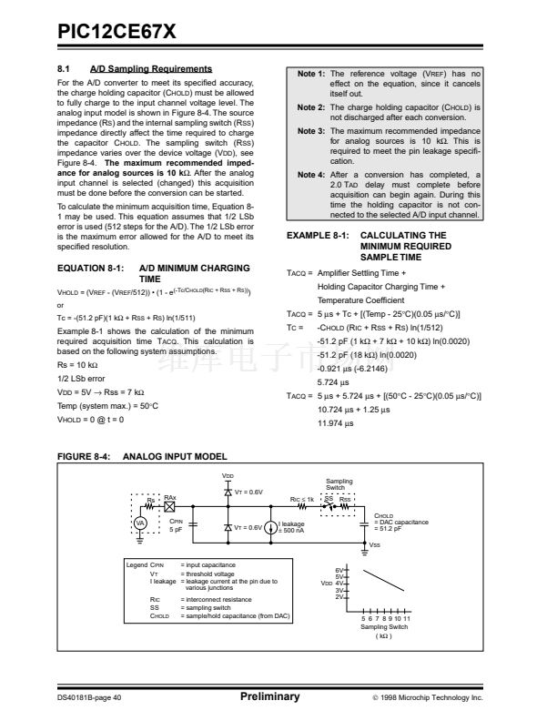
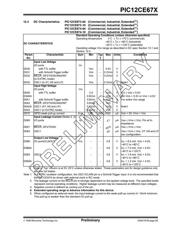
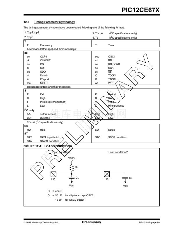
FIGURE 12-1: LOAD CONDITIONS
Load condition 1
V
DD
/2
Load condition 2
R
L
Pin
V
SS
R
L
= 464鈩?/div>
C
L
= 50 pF
15 pF
C
L
Pin
V
SS
C
L
for all pins except OSC2
for OSC2 output
漏
1998 Microchip Technology Inc.
Preliminary
DS40181B-page 89


 1
1
 2
2
 3
3
 4
4
 5
5
 6
6
 7
7
 8
8
 9
9
 10
10
 11
11
 12
12
 13
13
 14
14
 15
15
 16
16
 17
17
 18
18
 19
19
 20
20
 21
21
 22
22
 23
23
 24
24
 25
25
 26
26
 27
27
 28
28
 29
29
 30
30
 31
31
 32
32
 33
33
 34
34
 35
35
 36
36
 37
37
 38
38
 39
39
 40
40
 41
41
 42
42
 43
43
 44
44
 45
45
 46
46
 47
47
 48
48
 49
49
 50
50
 51
51
 52
52
 53
53
 54
54
 55
55
 56
56
 57
57
 58
58
 59
59
 60
60
 61
61
 62
62
 63
63
 64
64
 65
65
 66
66
 67
67
 68
68
 69
69
 70
70
 71
71
 72
72
 73
73
 74
74
 75
75
 76
76
 77
77
 78
78
 79
79
 80
80
 81
81
 82
82
 83
83
 84
84
 85
85
 86
86
 87
87
 88
88
 89
89
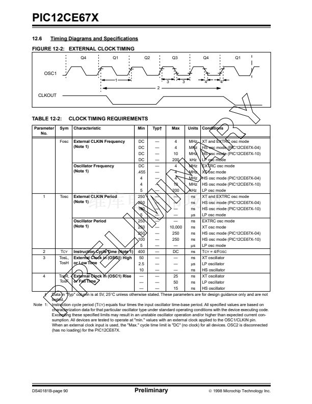 90
90
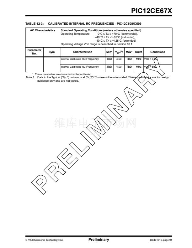 91
91
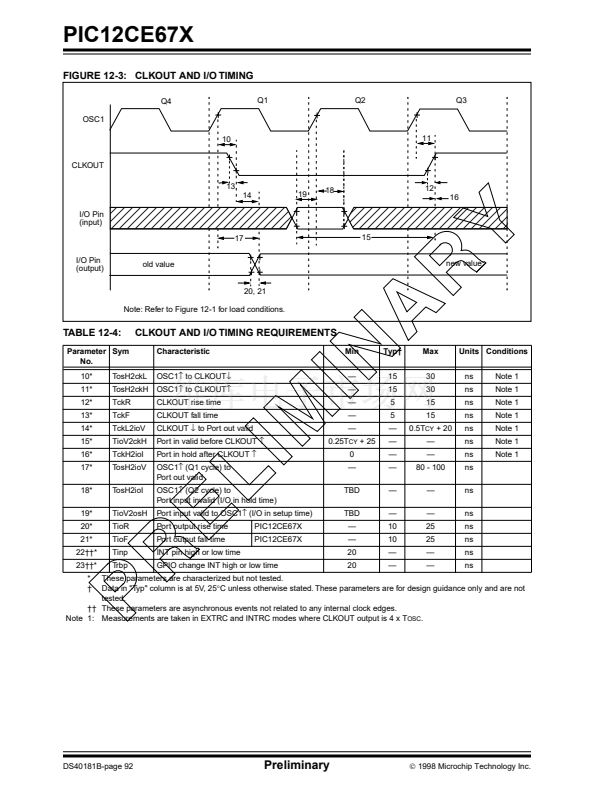 92
92
 93
93
 94
94
 95
95
 96
96
 97
97
 98
98
 99
99
 100
100
 101
101
 102
102
 103
103
 104
104
 105
105
 106
106
 107
107
 108
108
 109
109
 110
110
 111
111
 112
112
 113
113
 114
114
 115
115
 116
116
