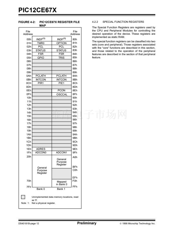
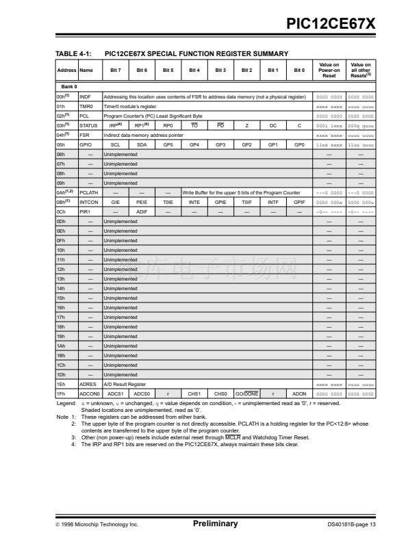
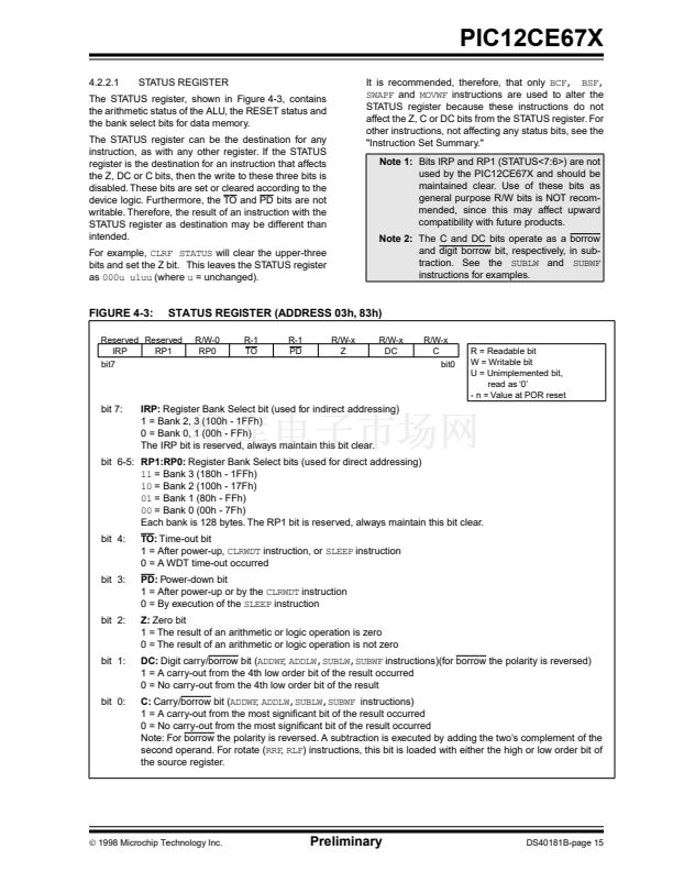
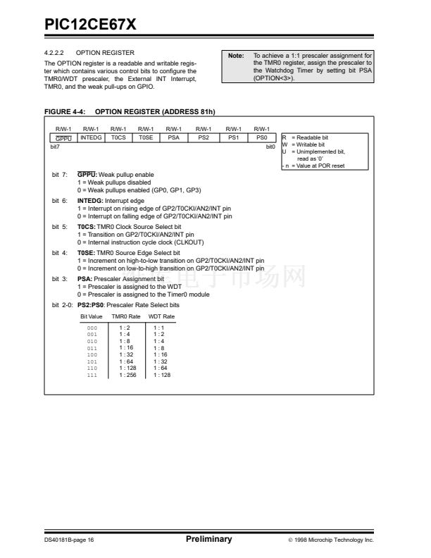
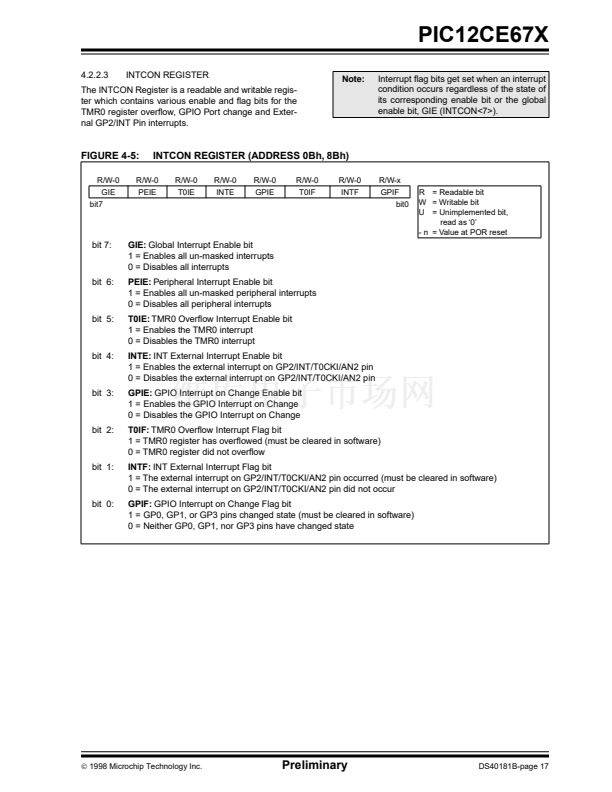
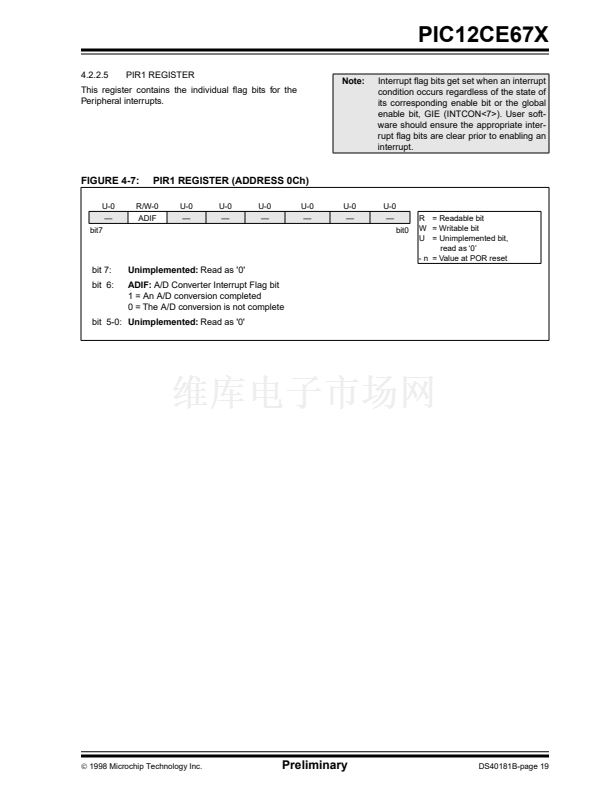
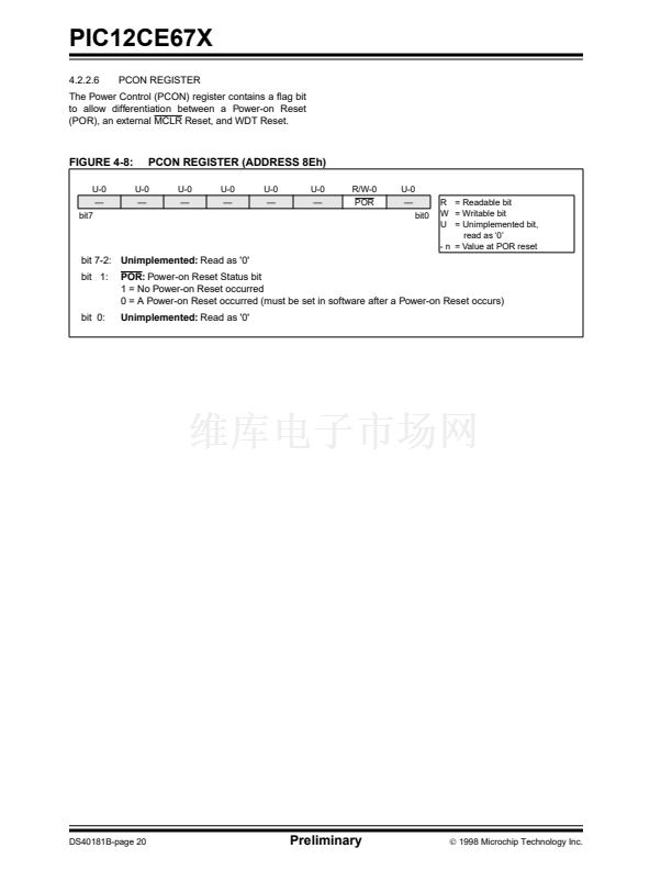
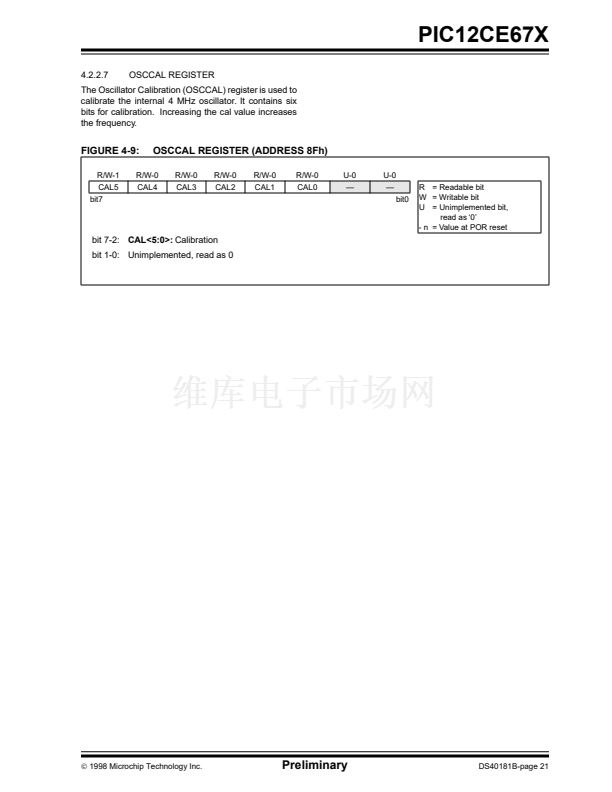
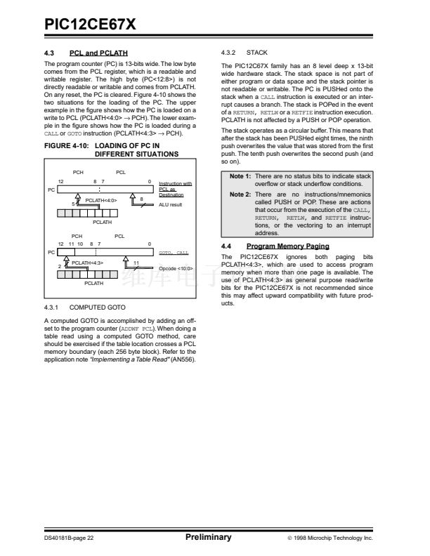
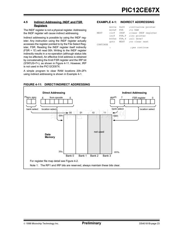
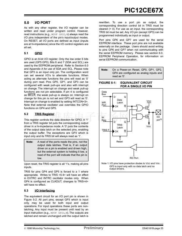
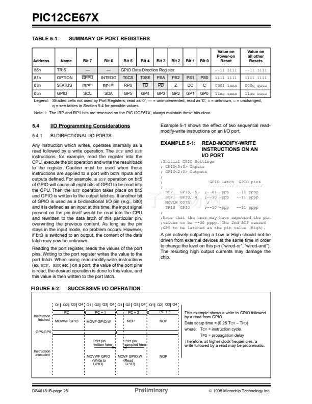
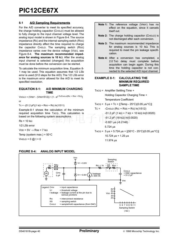
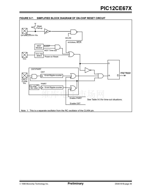
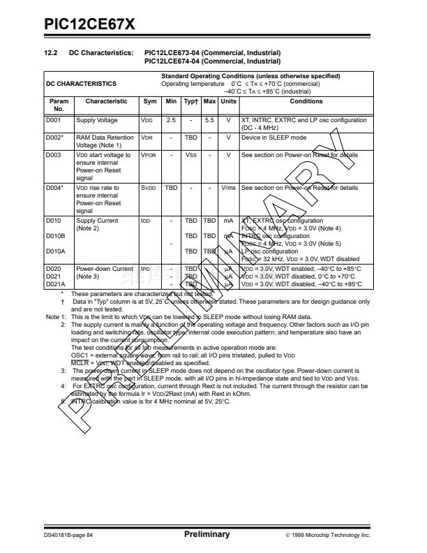
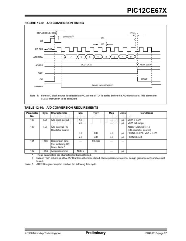
鈥?/div>
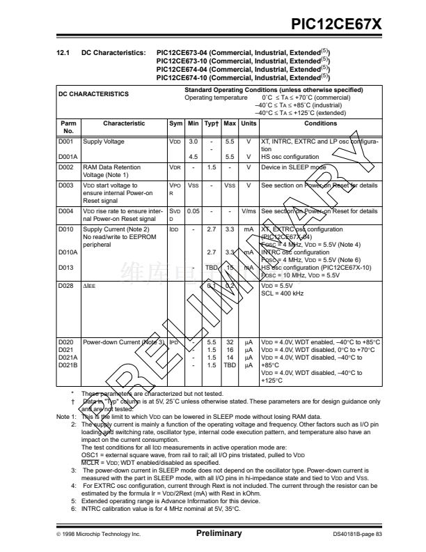
TBD
TBD
碌A
mA
碌A
Average current consumption when
A/D is on. (Note 2)
During sampling
All other times
These parameters are characterized but not tested.
Data in 鈥淭yp鈥?column is at 5V, 25掳C unless otherwise stated. These parameters are for design guidance only and are not
tested.
Note 1: These speci铿乧ations apply if V
REF
= 3.0V and if V
DD
鈮?/div>
3.0V. V
IN
must be between V
SS
and V
REF
2: When A/D is off, it will not consume any current other than minor leakage current. The power-down current spec includes
any such leakage from the A/D module.
3: V
REF
current is from GP1 pin or V
DD
pin, whichever is selected as reference input.
4: When using external V
REF
, V
DD
must be greater than 3V for +1 LSB accuracy. If V
DD
is less than 3V, you
must use internal V
REF
for +1 LSB.
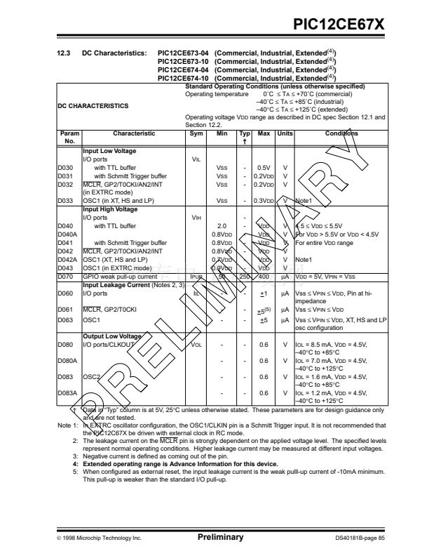
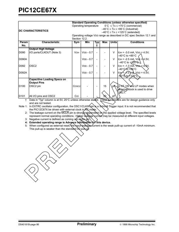
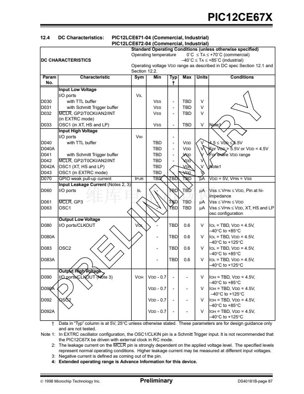
DS40181B-page 96
Preliminary
漏
1998 Microchip Technology Inc.


 1
1
 2
2
 3
3
 4
4
 5
5
 6
6
 7
7
 8
8
 9
9
 10
10
 11
11
 12
12
 13
13
 14
14
 15
15
 16
16
 17
17
 18
18
 19
19
 20
20
 21
21
 22
22
 23
23
 24
24
 25
25
 26
26
 27
27
 28
28
 29
29
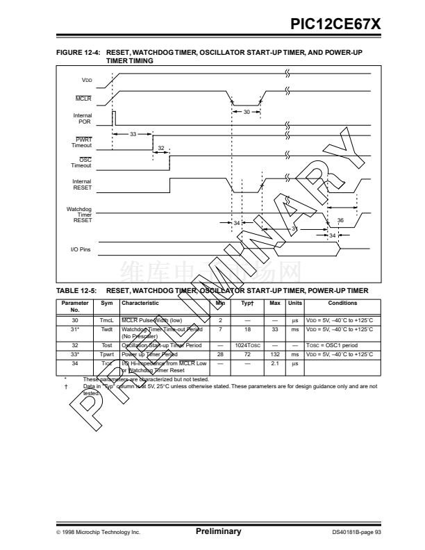
 30
30
 31
31
 32
32
 33
33
 34
34
 35
35
 36
36
 37
37
 38
38
 39
39
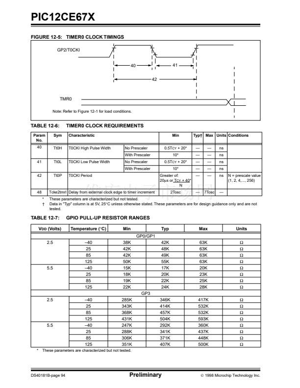
 40
40
 41
41
 42
42
 43
43
 44
44
 45
45
 46
46
 47
47
 48
48
 49
49
 50
50
 51
51
 52
52
 53
53
 54
54
 55
55
 56
56
 57
57
 58
58
 59
59
 60
60
 61
61
 62
62
 63
63
 64
64
 65
65
 66
66
 67
67
 68
68
 69
69
 70
70
 71
71
 72
72
 73
73
 74
74
 75
75
 76
76
 77
77
 78
78
 79
79
 80
80
 81
81
 82
82
 83
83
 84
84
 85
85
 86
86
 87
87
 88
88
 89
89
 90
90
 91
91
 92
92
 93
93
 94
94
 95
95
 96
96
 97
97
 98
98
 99
99
 100
100
 101
101
 102
102
 103
103
 104
104
 105
105
 106
106
 107
107
 108
108
 109
109
 110
110
 111
111
 112
112
 113
113
 114
114
 115
115
 116
116
