2SK2627
Continued from preceding page.
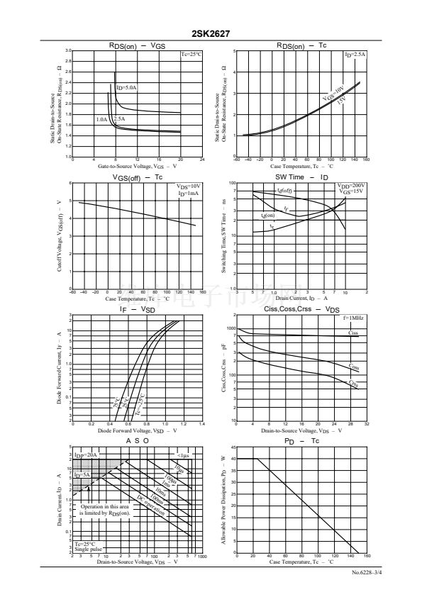
Parameter
Total Gate Charge
Turn-ON Delay Time
Rise Time
Turn-OFF Delay Time
Fall Time
Diode Forward Voltage
Symbol
Qg
td(on)
tr
td(off)
tf
VSD
Conditions
VDS=200V, VGS=10V, ID=5A
See specified Test Circuit
See specified Test Circuit
See specified Test Circuit
See specified Test Circuit
IS=5A, VGS=0
Ratings
min
typ
20
20
20
50
25
0.87
1.2
max
Unit
nC
ns
ns
ns
ns
V
Switching Time Test Circuit
VDD
=200V
15V
0V
VIN
VIN
D
PW=1碌s
D.C.鈮?.5%
G
ID
=2.5A
RL
=80.0鈩?/div>
VOUT
2SK2627
P.G
RGS
=50鈩?/div>
S
5
I D - VDS
15
V
10
I D - VDS
15V
4
10V
8V
8
10V
Drain Current, I
D
鈥?A
Drain Current, I
D
鈥?A
3
6
8V
7V
2
4
1
2
7V
VGS=6V
VGS=6V
0
0
2
4
6
8
10
0
0
10
20
30
40
50
Drain-to-Source Voltage, V
DS
鈥?V
8
7
6
5
4
3
2
1
0
0
Drain-to-Source Voltage, V
DS
鈥?V
10
ID - VGS
Forward Transfer Admittance, | yfs | 鈥?S
| y
f s
| - I
D
VDS=10V
VDS=10V
7
5
3
2
Tc=-25掳C
Drain Current, I
D
鈥?A
25
掳C
75掳C
C
25
掳
T
C
75
掳
c=-
1.0
7
5
3
2
25掳C
2
4
6
8
10
12
14
16
0.1
0.1
2
3
5
7
1.0
2
3
5
7
10
Gate-to-Source Voltage, V
GS
鈥?V
Drain Current, I
D
鈥?A
No.6228鈥?/4


 1
1
 2
2
 3
3
 4
4
