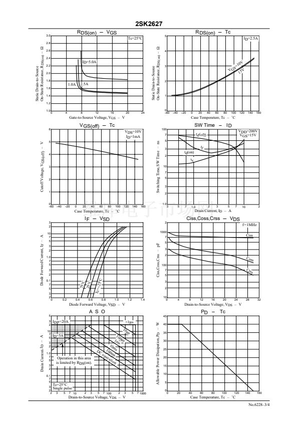
鈩?/div>
2.6
2.4
2.2
2.0
1.8
4
ID=5.0A
3
0V
=1
S
VG
V
15
2
1.0A
1.6
1.4
1.2
1.0
0
4
2.5A
1
8
12
16
20
24
0
-60
-40
-20
0
20
40
60
80
100
120
140
160
Gate-to-Source Voltage, V
GS
鈥?V
6
Case Temperature, Tc 鈥?藲C
V GS(off) - Tc
VDS=10V
ID=1mA
Switching Time, SW Time 鈥?ns
SW Time - I D
100
7
5
3
2
td (off)
tf
VDD=200V
VGS=15V
Cutoff Voltage, VGS(off) 鈥?V
5
4
td(on)
tr
3
10
7
5
3
2
2
1
0
-60
-40
-20
0
20
40
60
80
100
120
140
160
1.0
3
5
7
1.0
2
3
5
7
10
2
Case Temperature, Tc 鈥?藲C
3
2
Drain Current, I
D
鈥?A
2
1000
7
I F - VSD
Ciss,Coss,Crss - VDS
f=1MHz
Ciss
Diode Forward Current, I
F
鈥?A
10
7
5
3
2
1.0
7
5
3
2
0.1
7
5
3
2
Ciss,Coss,Crss 鈥?pF
5
3
2
100
7
5
3
2
10
0
Cos
s
Crs
s
75
掳
C
25
掳
C
0
0.2
0.4
0.6
Tc=-
0.8
25
掳
C
1.0
1.2
1.4
4
8
12
16
20
24
28
32
Diode Forward Voltage, VSD 鈥?V
Drain-to-Source Voltage, V
DS
鈥?V
45
A S O
5
PD - Tc
Allowable Power Dissipation, P
D
鈥?W
3
2
10
7
5
3
2
1.0
7
5
3
2
0.1
7
5
IDP=20A
ID=5A
10
<1碌s
10
碌
s
40
35
30
25
20
15
10
5
0
Drain Current, I
D
鈥?A
10
0
1m
碌
s
s
DC
Operation in this area
is limited by RDS(on).
ms
0m
op
era
s
tio
n
10
3
Single pulse
2
2 3
5 7 10
Tc=25掳C
2
3
5
7 100
2
3
5
7 1000
0
20
40
60
80
100
120
140
160
Drain-to-Source Voltage, V
DS
鈥?V
Case Temperature, Tc 鈥?藲C
No.6228鈥?/4


 1
1
 2
2
 3
3
 4
4
