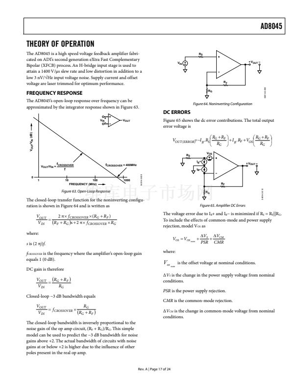
鈭?/div>
V
CM
+
PSR CMR
where:
V
os
nom
is the offset voltage at nominal conditions.
螖
V
S
is the change in the power supply voltage from nominal
conditions.
PSR
is the power supply rejection.
Closed-loop 鈭? dB bandwidth equals
V
OUT
R
G
=
f
CROSSOVER
脳
(
R
G
+
R
F
)
V
IN
C
MR
is the common-mode rejection.
螖
V
CM
is the change in common-mode voltage from nominal
conditions.
The closed-loop bandwidth is inversely proportional to the
noise gain of the op amp circuit, (R
F
+ R
G
)/R
G
. This simple
model can be used to predict the 鈭? dB bandwidth for noise
gains above +2. The actual bandwidth of circuits with noise
gains at or below +2 is higher due to the influence of other
poles present in the real op amp.
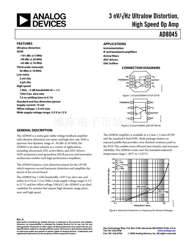
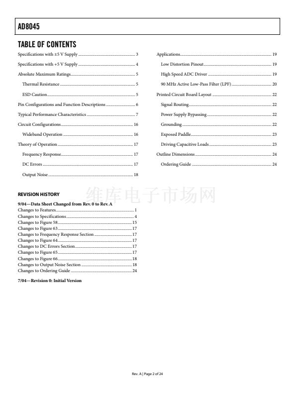
Rev. A | Page 17 of 24


 1
1
 2
2
 3
3
 4
4
 5
5
 6
6
 7
7
 8
8
 9
9
 10
10
 11
11
 12
12
 13
13
 14
14
 15
15
 16
16
 17
17
 18
18
 19
19
 20
20
 21
21
 22
22
 23
23
 24
24
