AD8045
TABLE OF CONTENTS
Specifications with 卤5 V Supply ..................................................... 3
Specifications with +5 V Supply ..................................................... 4
Absolute Maximum Ratings............................................................ 5
Thermal Resistance ...................................................................... 5
ESD Caution.................................................................................. 5
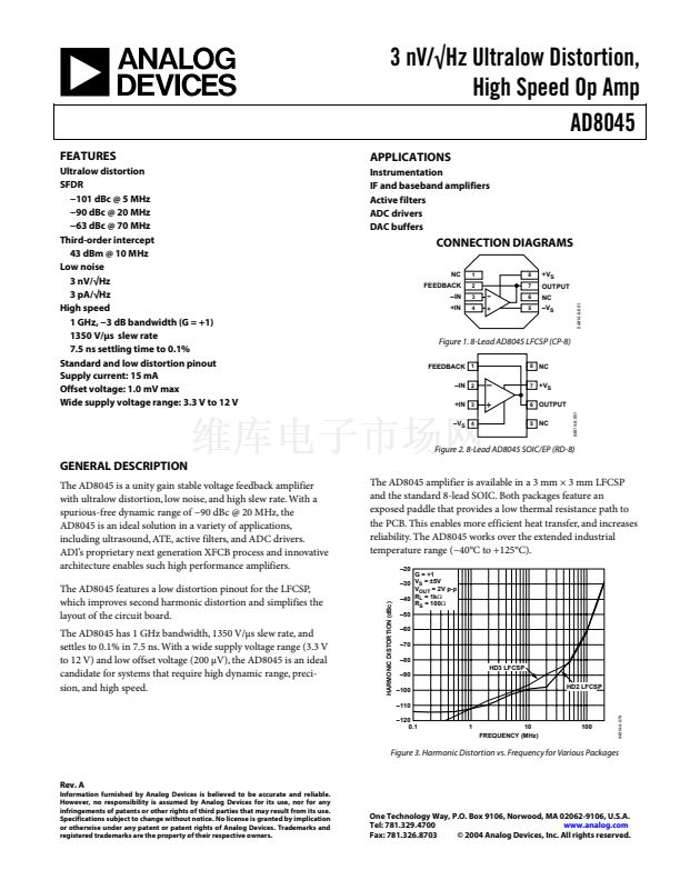
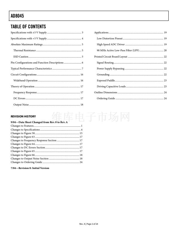
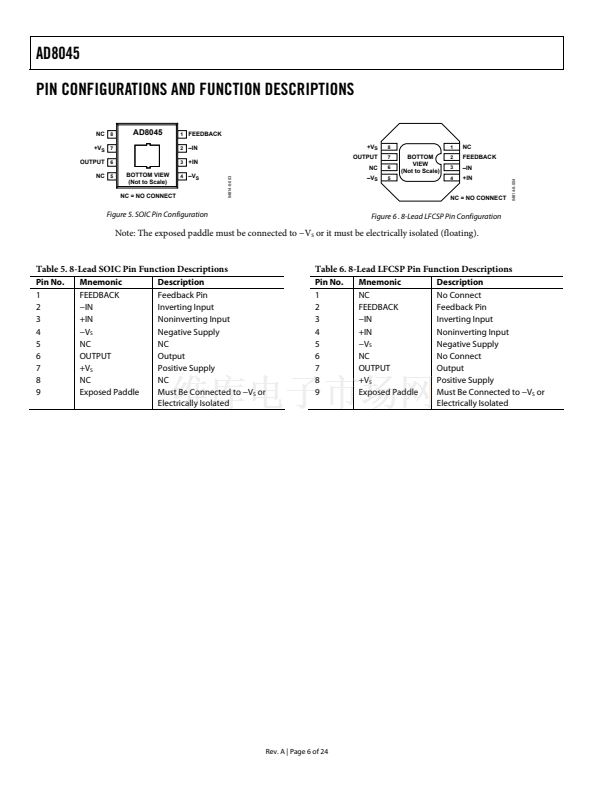
Pin Configurations and Function Descriptions ........................... 6
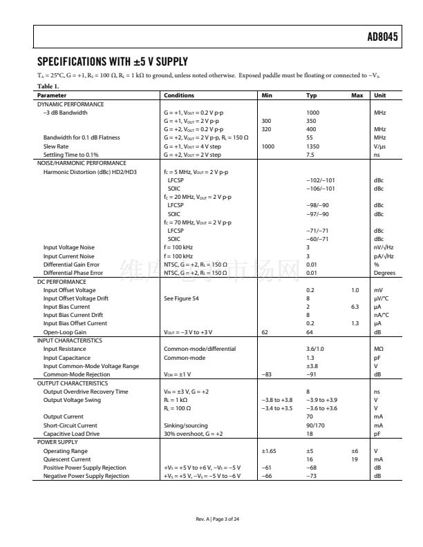
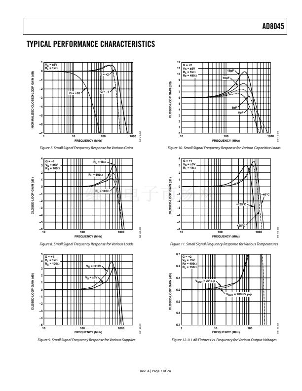
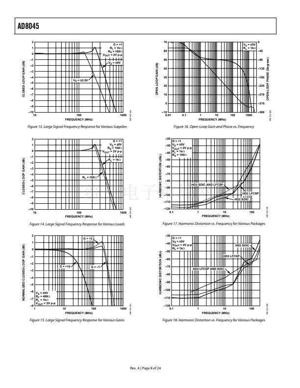
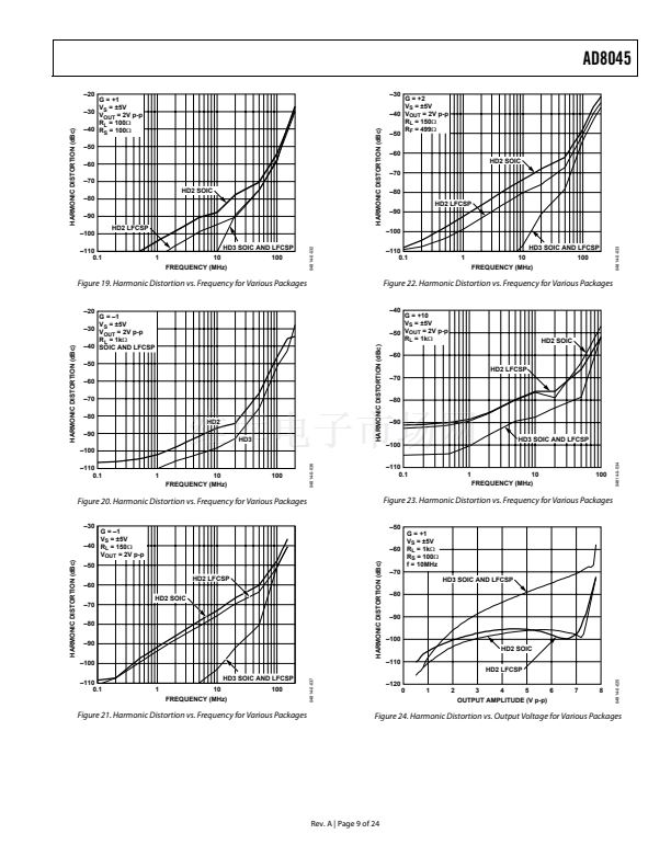
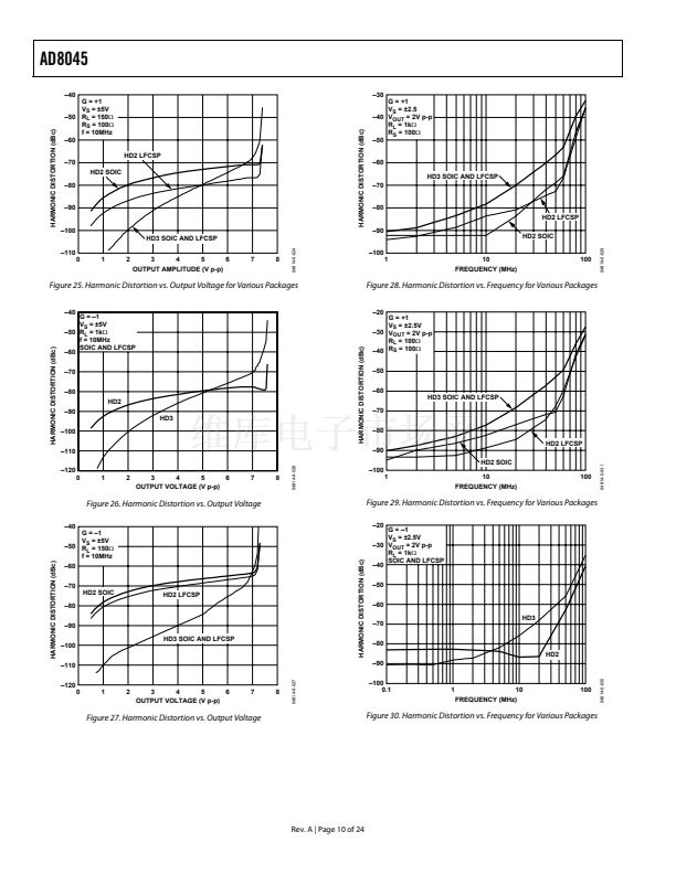
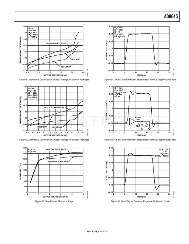
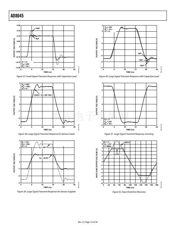
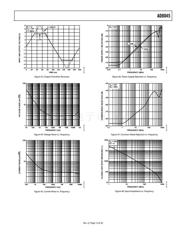
Typical Performance Characteristics ............................................. 7
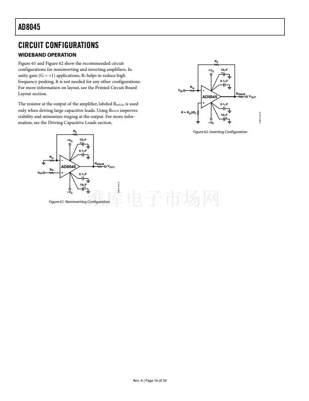
Circuit Configurations................................................................... 16
Wideband Operation ................................................................. 16
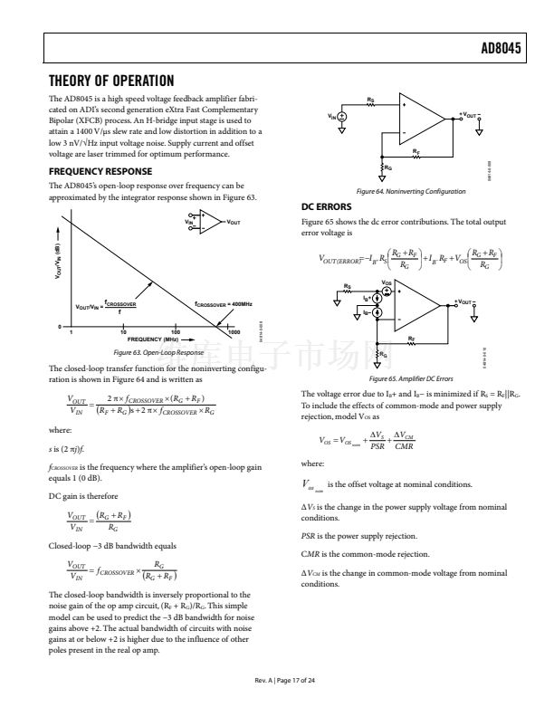
Theory of Operation ...................................................................... 17
Frequency Response................................................................... 17
DC Errors .................................................................................... 17
Output Noise............................................................................... 18
Applications..................................................................................... 19
Low Distortion Pinout............................................................... 19
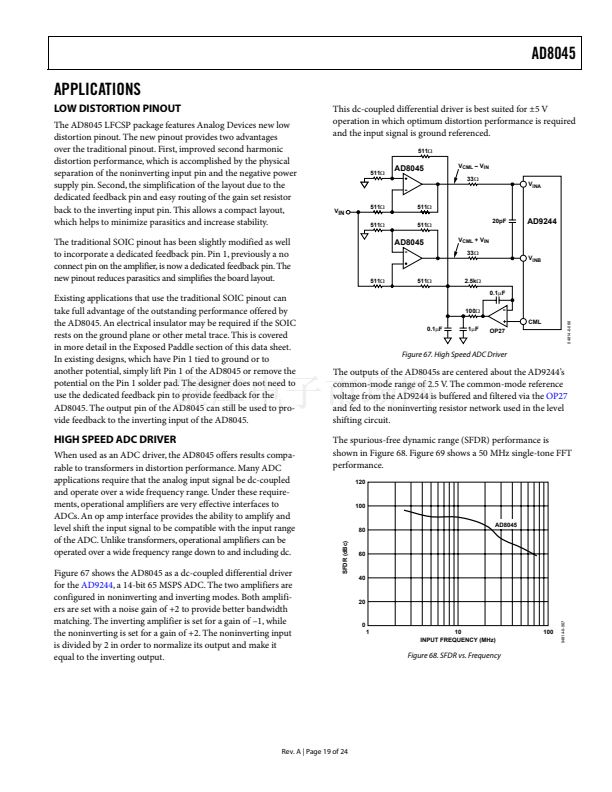
High Speed ADC Driver ........................................................... 19
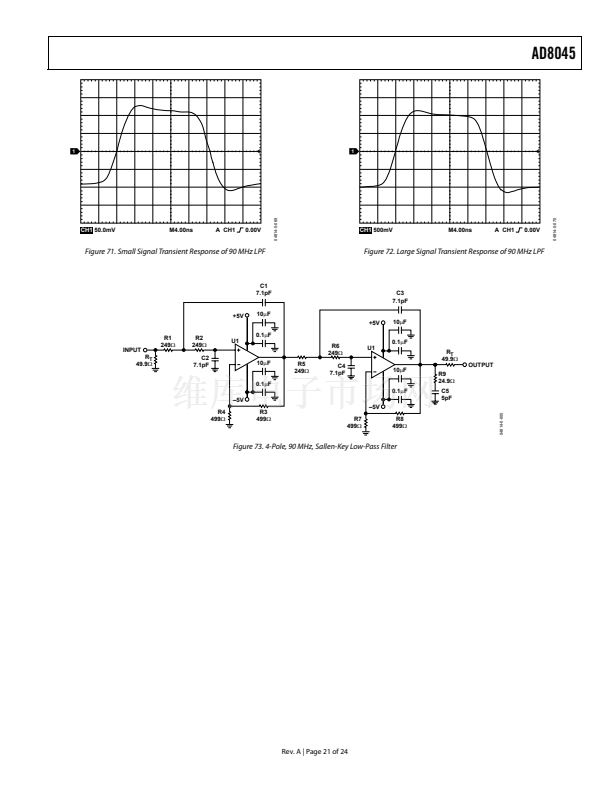
90 MHz Active Low-Pass Filter (LPF) ..................................... 20
Printed Circuit Board Layout ....................................................... 22
Signal Routing............................................................................. 22
Power Supply Bypassing ............................................................ 22
Grounding ................................................................................... 22
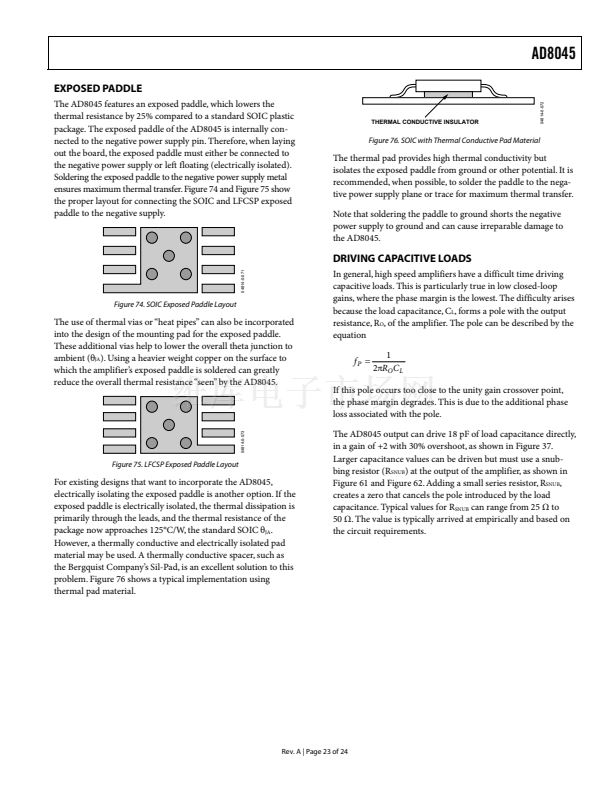
Exposed Paddle........................................................................... 23
Driving Capacitive Loads.......................................................... 23
Outline Dimensions ....................................................................... 24
Ordering Guide .......................................................................... 24
REVISION HISTORY
9/04鈥擠ata Sheet Changed from Rev. 0 to Rev. A
Changes to Features......................................................................... 1
Changes to Specifications ............................................................... 4
Changes to Figure 58..................................................................... 15
Changes to Figure 63..................................................................... 17
Changes to Frequency Response Section ................................... 17
Changes to Figure 64..................................................................... 17
Changes to DC Errors Section..................................................... 17
Changes to Figure 65..................................................................... 17
Changes to Figure 66..................................................................... 18
Changes to Output Noise Section ............................................... 18
Changes to Ordering Guide ......................................................... 24
7/04鈥擱evision 0: Initial Version
Rev. A | Page 2 of 24


 1
1
 2
2
 3
3
 4
4
 5
5
 6
6
 7
7
 8
8
 9
9
 10
10
 11
11
 12
12
 13
13
 14
14
 15
15
 16
16
 17
17
 18
18
 19
19
 20
20
 21
21
 22
22
 23
23
 24
24
