may cause permanent damage to the device. This is a stress
section of this specification is not implied. Exposure to absolute
device reliability.
RMS output voltages should be considered. If
鈭?/div>
V
S
, as in single-supply operation, the total drive power is
V
S
脳
I
OUT
. If the rms signal levels are indeterminate, consider the
worst case, when
V
OUT
=
V
S
/4 for
R
L
to midsupply.
(
V
S
/
4
)
2
P
D
=
(
V
S
脳
I
S
)
+
R
L
In single-supply operation with
R
L
referenced to 鈭扸
S
, worst case
is
V
OUT
=
V
S
/2.
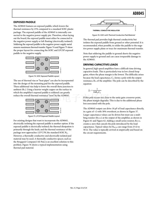
Airflow increases heat dissipation, effectively reducing 胃
JA
.
Also, more metal directly in contact with the package leads and
exposed paddle from metal traces, through holes, ground, and
power planes reduce 胃
JA
.
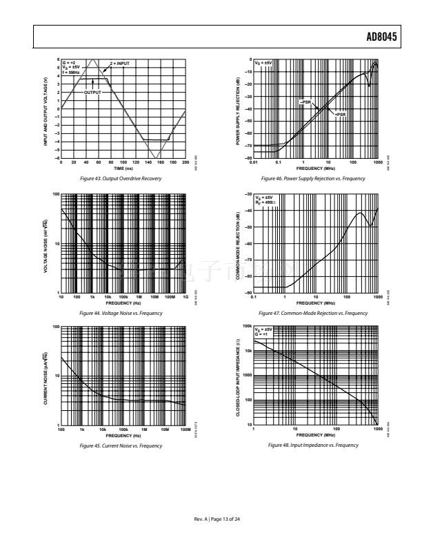
Figure 4 shows the maximum safe power dissipation in the
package versus the ambient temperature for the exposed paddle
SOIC (80掳C/W) and LFCSP (93掳C/W) package on a JEDEC
standard 4-layer board. 胃
JA
values are approximations.
4.0
THERMAL RESISTANCE
胃
JA
is specified for the worst-case conditions, i.e., 胃
JA
is specified
for device soldered in circuit board for surface-mount packages.
Table 4. Thermal Resistance
Package Type
SOIC
LFCSP
胃
JA
80
93
胃
JC
30
35
Unit
掳C/W
掳C/W
Maximum Power Dissipation
The maximum safe power dissipation for the AD8045 is limited
by the associated rise in junction temperature (T
J
) on the die. At
approximately 150掳C, which is the glass transition temperature,
the properties of the plastic change. Even temporarily exceeding
this temperature limit may change the stresses that the package
exerts on the die, permanently shifting the parametric perform-
ance of the AD8045. Exceeding a junction temperature of
175掳C for an extended period of time can result in changes in
silicon devices, potentially causing degradation or loss of
functionality.
MAXIMUM POWER DISSIPATION (Watts)
3.5
3.0
2.5
2.0
1.5
1.0
LFCSP
0.5
0.0
鈥?0
04814-0-080
SOIC
鈥?0
0
20
40
60
80
AMBIENT TEMPERATURE (掳C)
100
120
Figure 4. Maximum Power Dissipation vs. Temperature for a 4-Layer Board
ESD CAUTION
ESD (electrostatic discharge) sensitive device. Electrostatic charges as high as 4000 V readily accumulate
on the human body and test equipment and can discharge without detection. Although this product features
proprietary ESD protection circuitry, permanent damage may occur on devices subjected to high energy elec-
trostatic discharges. Therefore, proper ESD precautions are recommended to avoid performance degradation
and loss of functionality.
Rev. A | Page 5 of 24


 1
1
 2
2
 3
3
 4
4
 5
5
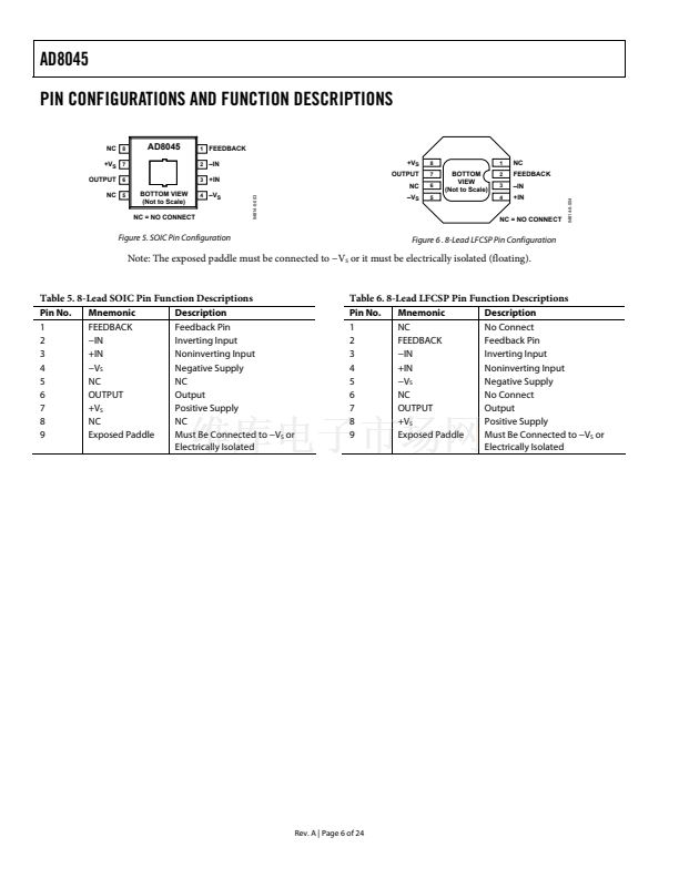 6
6
 7
7
 8
8
 9
9
 10
10
 11
11
 12
12
 13
13
 14
14
 15
15
 16
16
 17
17
 18
18
 19
19
 20
20
 21
21
 22
22
 23
23
 24
24
