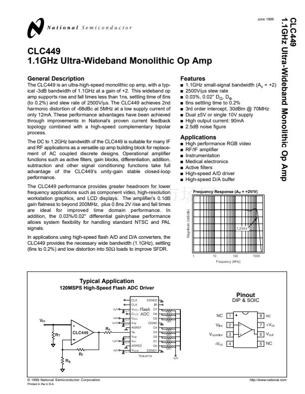
鈥?/div>
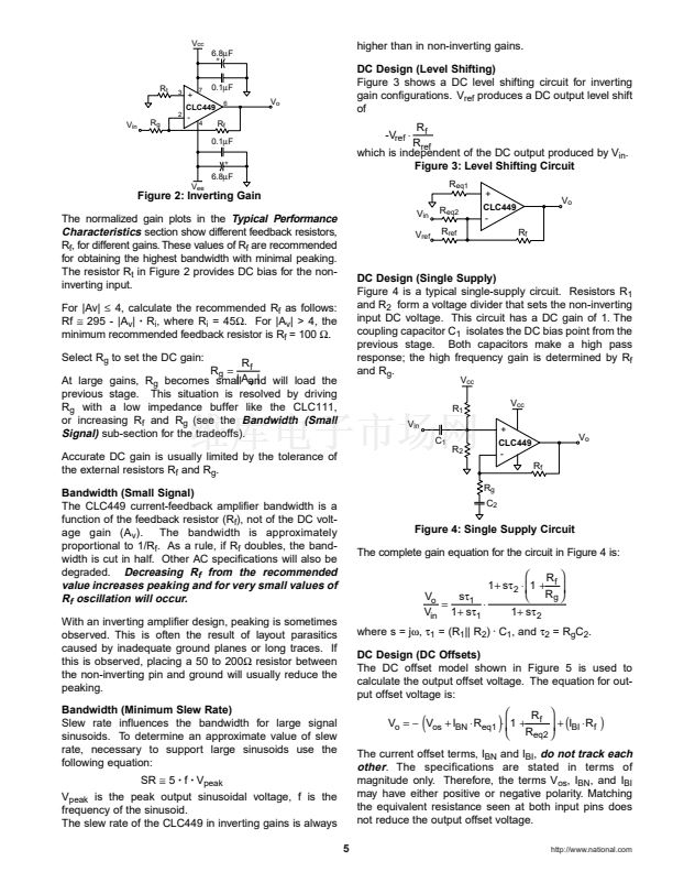
R
i
, where R
i
= 45鈩? For |A
v
| > 4, the
minimum recommended feedback resistor is R
f
= 100
鈩?
R
f
R
g
=
|
v
|
At large gains, R
g
becomes smallAand will load the
previous stage. This situation is resolved by driving
R
g
with a low impedance buffer like the CLC111,
or increasing R
f
and R
g
(see the
Bandwidth (Small
Signal)
sub-section for the tradeoffs).
Accurate DC gain is usually limited by the tolerance of
the external resistors R
f
and R
g
.
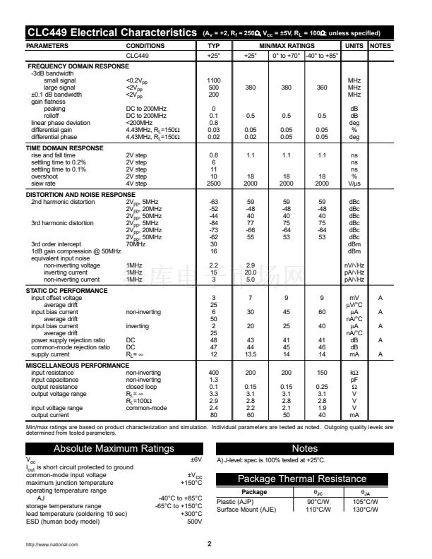
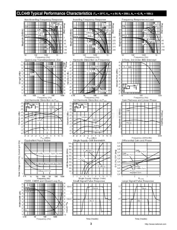
Bandwidth (Small Signal)
The CLC449 current-feedback amplifier bandwidth is a
function of the feedback resistor (R
f
), not of the DC volt-
age gain (A
v
). The bandwidth is approximately
proportional to 1/R
f
. As a rule, if R
f
doubles, the band-
width is cut in half. Other AC specifications will also be
degraded.
Decreasing R
f
from the recommended
value increases peaking and for very small values of
R
f
oscillation will occur.
With an inverting amplifier design, peaking is sometimes
observed. This is often the result of layout parasitics
caused by inadequate ground planes or long traces. If
this is observed, placing a 50 to 200鈩?resistor between
the non-inverting pin and ground will usually reduce the
peaking.
Bandwidth (Minimum Slew Rate)
Slew rate influences the bandwidth for large signal
sinusoids. To determine an approximate value of slew
rate, necessary to support large sinusoids use the
following equation:
SR
鈮?/div>
5
鈥?/div>
f
鈥?/div>
V
peak
V
peak
is the peak output sinusoidal voltage, f is the
frequency of the sinusoid.
The slew rate of the CLC449 in inverting gains is always
5
Select R
g
to set the DC gain:
R
eq2
R
ref
V
ee
V
o
R
f
-
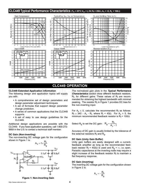
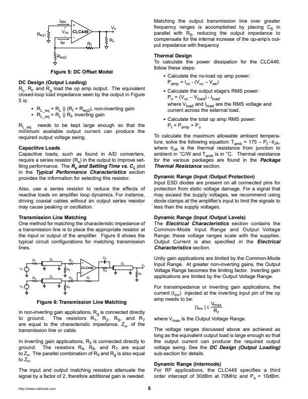
DC Design (Single Supply)
Figure 4 is a typical single-supply circuit. Resistors R
1
and R
2
form a voltage divider that sets the non-inverting
input DC voltage. This circuit has a DC gain of 1. The
coupling capacitor C
1
isolates the DC bias point from the
previous stage. Both capacitors make a high pass
response; the high frequency gain is determined by R
f
and R
g
.
V
cc
R
1
V
in
C
1
R
2
+
CLC449
V
cc
V
o
R
f
-
R
g
C
2
Figure 4: Single Supply Circuit
The complete gain equation for the circuit in Figure 4 is:
铮?/div>
R
铮?/div>
1
+
s
蟿
2
鈰?铮?/div>
1
+
f
铮?/div>
铮?/div>
R
g
铮?/div>
s
蟿
1
V
o
=
鈰?/div>
V
in
1
+
s
蟿
1
1
+
s
蟿
2
where s = j蠅,
蟿
1
= (R
1
|| R
2
)
鈥?/div>
C
1
, and
蟿
2
= R
g
C
2
.
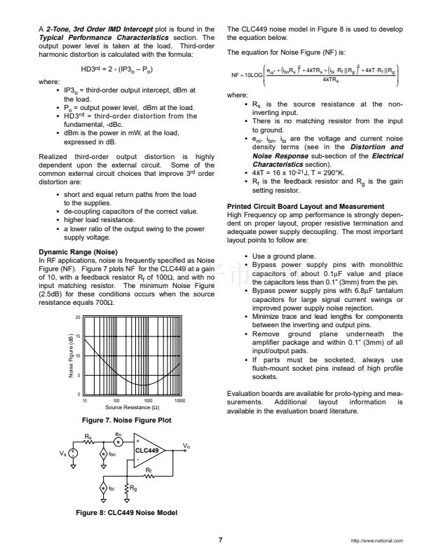
DC Design (DC Offsets)
The DC offset model shown in Figure 5 is used to
calculate the output offset voltage. The equation for out-
put offset voltage is:
铮?/div>
R
f
铮?/div>
V
o
= 鈭?/div>
V
os
+
I
BN
鈰?/div>
R
eq1
鈰?铮?/div>
1
+
铮?+
(
I
BI
鈰?/div>
R
f
)
铮?/div>
R
eq2
铮?/div>
(
)
The current offset terms, I
BN
and I
BI
,
do not track each
other
. The specifications are stated in terms of
magnitude only. Therefore, the terms V
os
, I
BN
, and I
BI
may have either positive or negative polarity. Matching
the equivalent resistance seen at both input pins does
not reduce the output offset voltage.
http://www.national.com
CLC449AJE相关型号PDF文件下载
-
型号
版本
描述
厂商
下载
-
英文版
Fllstandssensoren Schaltverstarker Baureihe CLC
ETC
-
英文版
Fllstandssensoren Schaltverstarker Baureihe CLC
ETC [ETC]
-
英文版
Fast Settling, Wideband Low-Gain Monolithic Op Amp
NSC
-
英文版
Fast Settling, Wideband Low-Gain Monolithic Op Amp
NSC [Natio...
-
英文版
Fast Settling, Wideband High-Gain Monolithic Op Amp
NSC
-
英文版
Fast Settling, Wideband High-Gain Monolithic Op Amp
NSC [Natio...
-
英文版
Low-Gain Op Amp with Fast 14-Bit Settling
NSC
-
英文版
Low-Gain Op Amp with Fast 14-Bit Settling
NSC [Natio...
-
英文版
Wideband, High-Slew Rate, Monolithic Op Amp
NSC
-
英文版
Wideband, High-Slew Rate, Monolithic Op Amp
NSC [Natio...
-
英文版
Low-Cost, Low-Power, 110MHz Op Amp with Disable
NSC
-
英文版
Low-Cost, Low-Power, 110MHz Op Amp with Disable
NSC [Natio...
-
英文版
Wideband, Low Power Monolithic Op Amp
NSC
-
英文版
Wideband, Low Power Monolithic Op Amp
NSC [Natio...
-
英文版
Low-Cost, Low-Power Programmable Gain Buffer with Disable
NSC
-
英文版
Low-Cost, Low-Power Programmable Gain Buffer with Disable
NSC [Natio...
-
英文版
Comlinear CLC408 High-Speed, Low-Power Line Driver
NSC
-
英文版
Comlinear CLC408 High-Speed, Low-Power Line Driver
NSC [Natio...
-
英文版
Very Wideband, Low Distortion Monolithic Op Amp
NSC
-
英文版
Very Wideband, Low Distortion Monolithic Op Amp
NSC [Natio...


 1
1
 2
2
 3
3
 4
4
 5
5
 6
6
 7
7
 8
8
 9
9
 10
10
 11
11
 12
12
