鈥?/div>
胃
JA
,
where
胃
JA
is the thermal resistance from junction to
ambient in 掳C/W and T
amb
is in 掳C. Thermal resistance
for the various packages are found in the
Package
Thermal Resistance
section.
Dynamic Range (Input /Output Protection)
Input ESD diodes are present on all connected pins for
protection from static voltage damage. For a signal that
may exceed the supply voltages, we recommend using
diode clamps at the amplifier鈥檚 input to limit the signals to
less than the supply voltages.
Dynamic Range (Input /Output Levels)
The
Electrical Characteristics
section contains the
Common-Mode Input Range and Output Voltage
Range; these voltage ranges scale with the supplies.
Output Current is also specified in the
Electrical
Characteristics
section.
Unity gain applications are limited by the Common-Mode
Input Range. At greater non-inverting gains, the Output
Voltage Range becomes the limiting factor. Inverting gain
applications are limited by the Output Voltage Range.
For transimpedance or inverting gain applications, the
current (I
inv
) injected at the inverting input pin of the op
amp needs to be:
V
|I
inv
|
鈮?/div>
max
R
f
where V
max
is the Output Voltage Range.
The voltage ranges discussed above are achieved as
long as the equivalent output load is large enough so that
the output current can produce the required output
voltage swing. See the
DC Design (Output Loading)
sub-section for details.
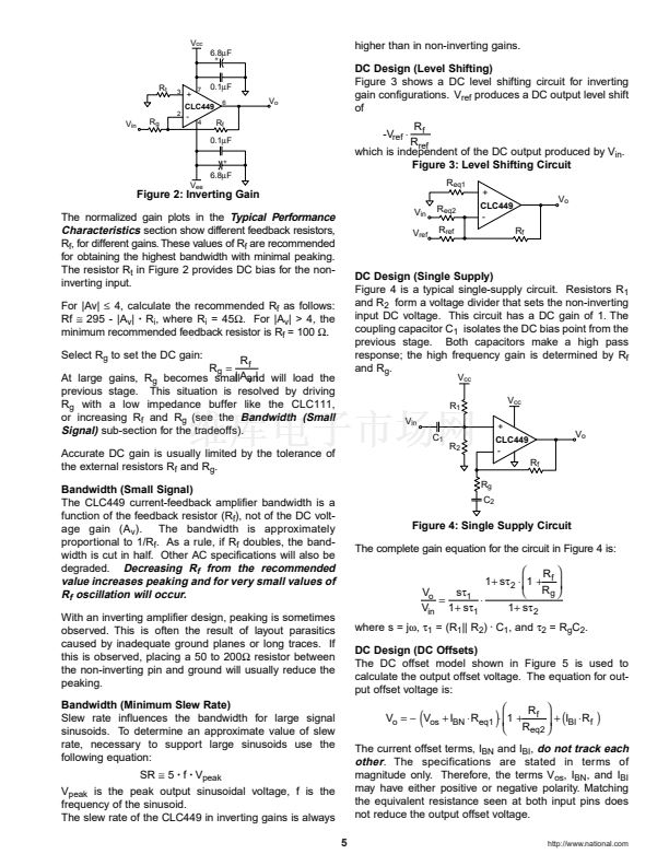
Dynamic Range (Intermods)
For RF applications, the CLC449 specifies a third
order intercept of 30dBm at 70MHz and P
o
= 10dBm.
6
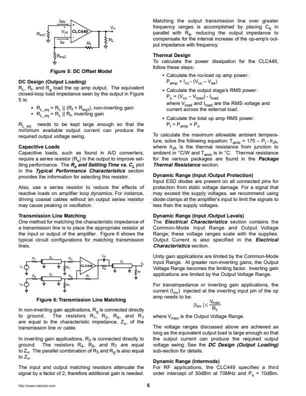
Z
0
R
6
CLC449
-
V
o
R
7
R
f
Figure 6: Transmission Line Matching
In non-inverting gain applications, R
g
is connected directly
to ground.
The resistors R
1
, R
2
, R
6
, and R
7
are equal to the characteristic impedance, Z
o
, of the
transmission line or cable.
In inverting gain applications, R
3
is connected directly to
ground. The resistors R
4
, R
6
, and R
7
are equal
to Z
o
. The parallel combination of R
5
and R
g
is also equal
to Z
o
.
The input and output matching resistors attenuate the
signal by a factor of 2, therefore additional gain is needed.
http://www.national.com


 1
1
 2
2
 3
3
 4
4
 5
5
 6
6
 7
7
 8
8
 9
9
 10
10
 11
11
 12
12
