CS8415A
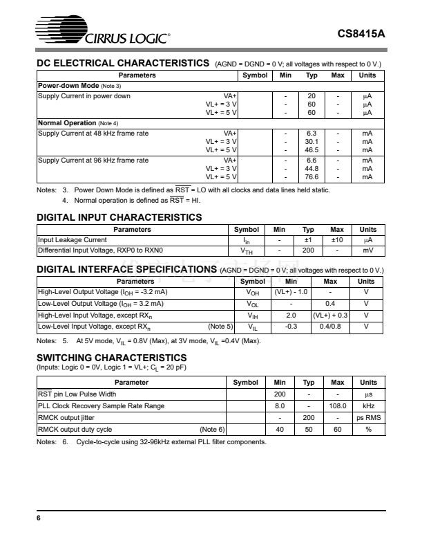
7. CONTROL PORT REGISTER SUMMARY
Addr
(HEX)
01
02
04
06
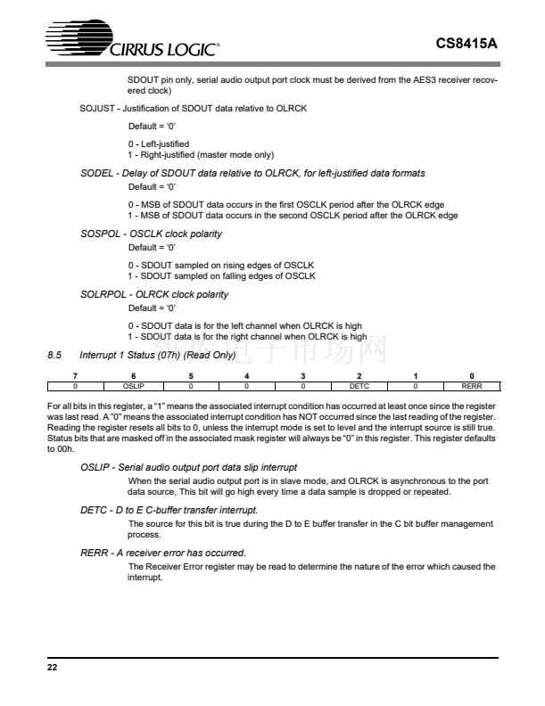
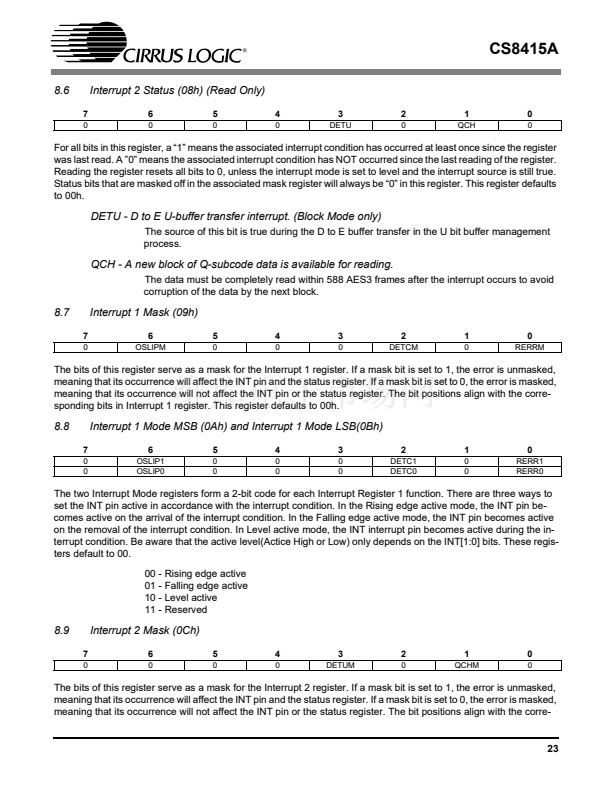
07
08
09
0A
0B
0C
0D
0E
0F
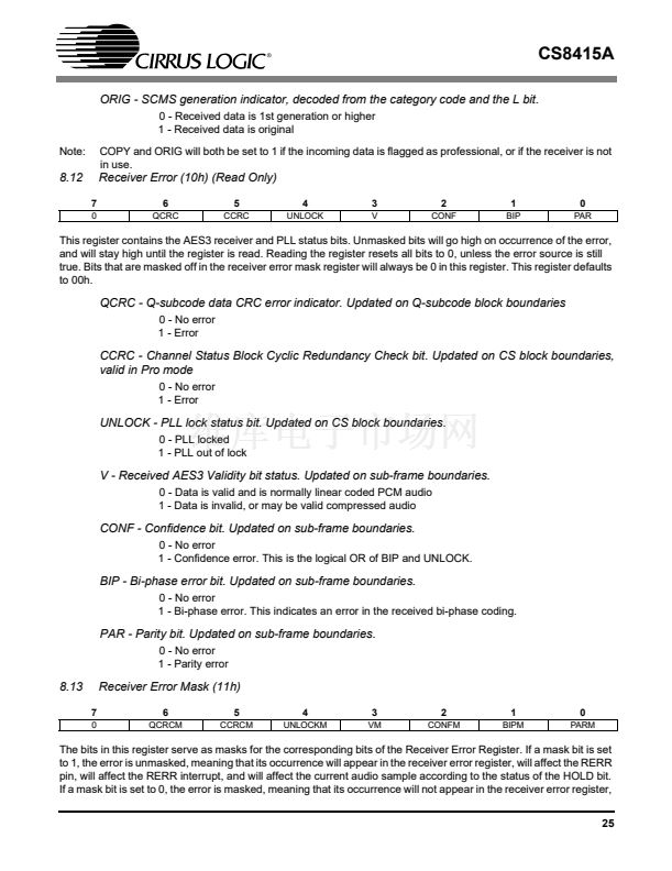
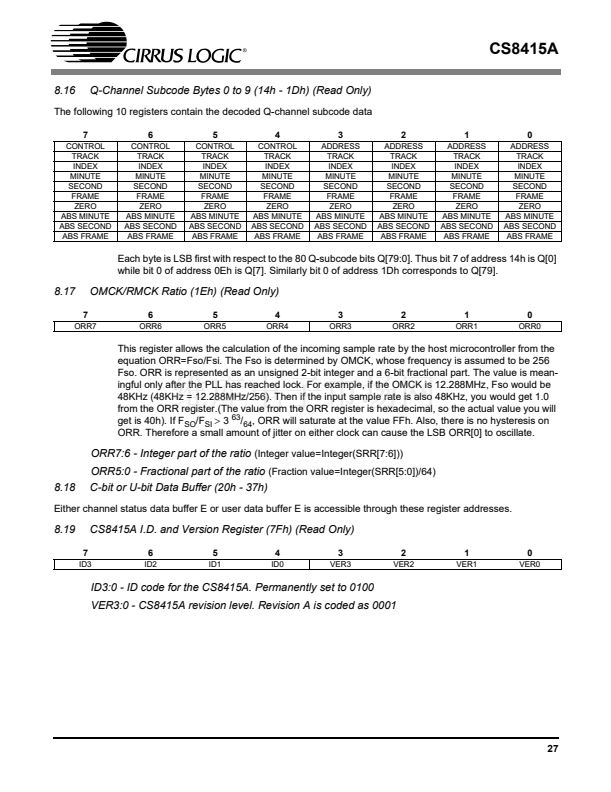
10
11
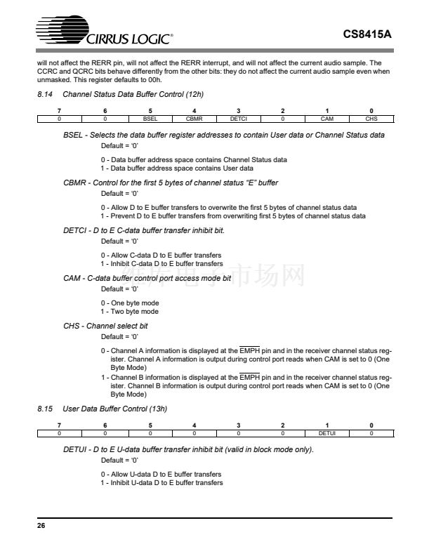
12
13
14-1D
1E
20-37
7F
Function
Control 1
Control 2
Clock Source Control
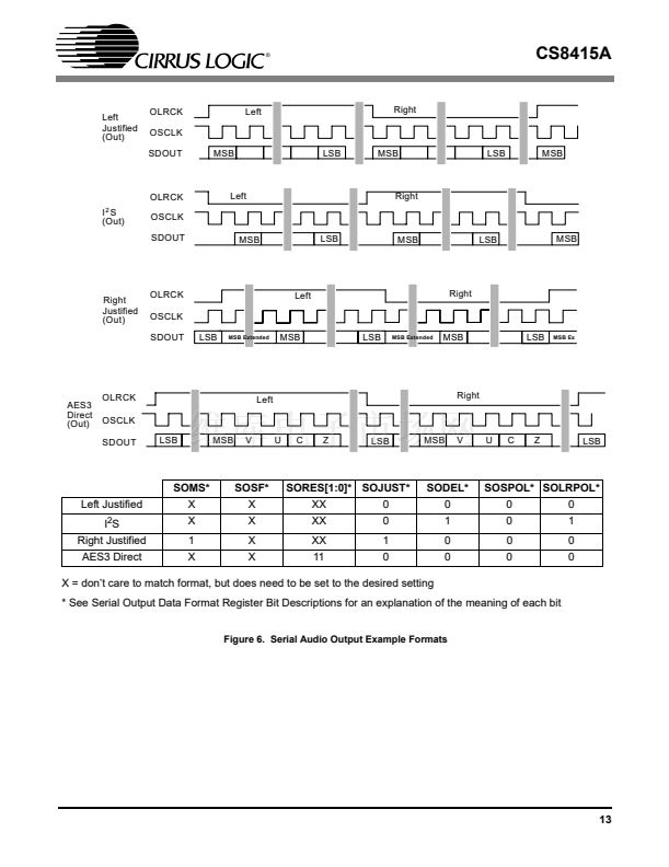
Serial Output Format
Interrupt 1 Status
Interrupt 2 Status
Interrupt 1 Mask
Interrupt 1 Mode (MSB)
Interrupt 1 Mode (LSB)
Interrupt 2 Mask
Interrupt 2 Mode (MSB)
Interrupt 2 Mode (LSB)
Receiver CS Data
Receiver Errors
Receiver Error Mask
CS Data Buffer Control
U Data Buffer Control
Q sub-code Data
OMCK/RMCK Ratio
C or U Data Buffer
ID and Version
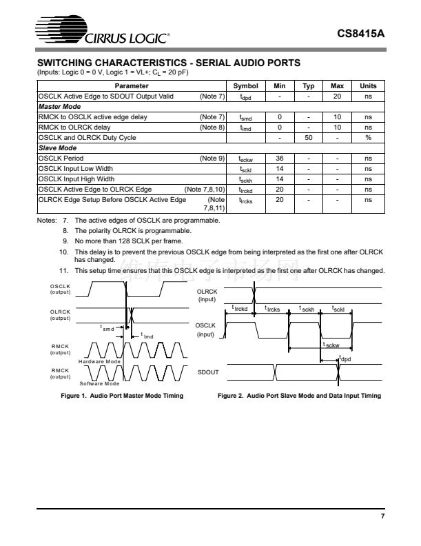
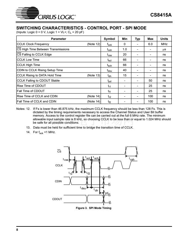
7
SWCLK
0
0
SOMS
0
0
0
0
0
0
0
0
AUX3
0
0
0
0
6
0
HOLD1
RUN
SOSF
OSLIP
0
OSLIPM
OSLIP1
OSLIP0
0
0
0
AUX2
QCRC
QCRCM
0
0
5
MUTESAO
HOLD0
0
SORES1
0
0
0
0
0
0
0
0
AUX1
CCRC
CCRCM
BSEL
0
4
0
RMCKF
0
SORES0
0
0
0
0
0
0
0
0
AUX0
UNLOCK
UNLOCKM
CBMR
0
3
0
MMR
0
SOJUST
0
DETU
0
0
0
DETUM
DETU1
DETU0
PRO
V
VM
DETCI
0
2
INT1
MUX2
0
SODEL
DETC
0
DETCM
DETC1
DETC0
0
0
0
AUDIO
CONF
CONFM
0
0
1
INT0
MUX1
0
SOSPOL
0
QCH
0
0
0
QCHM
QCH1
QCH0
COPY
BIP
BIPM
CAM
DETUI
0
0
MUX0
1
SOLRPOL
RERR
0
RERRM
RERR1
RERR0
0
0
0
ORIG
PAR
PARM
CHS
0
ORR7
ORR6
ORR5
ORR4
ORR3
ORR2
ORR1
ORR0
ID3
ID2
ID1
ID0
VER3
VER2
VER1
VER0
Table 1. Control Register Map Summary
7.1
Memory Address Pointer (MAP)
7
INCR
6
MAP6
5
MAP5
4
MAP4
3
MAP3
2
MAP2
1
MAP1
0
MAP0
INCR - Auto Increment Address Control Bit
Default = 鈥?鈥?/div>
0 - Disabled
1 - Enabled
MAP6:MAP0 - Register address
Note:
Reserved registers must not be written to during normal operation. Some reserved registers are used for
test modes, which can completely alter the normal operation of the CS8415A.
19


 1
1
 2
2
 3
3
 4
4
 5
5
 6
6
 7
7
 8
8
 9
9
 10
10
 11
11
 12
12
 13
13
 14
14
 15
15
 16
16
 17
17
 18
18
 19
19
 20
20
 21
21
 22
22
 23
23
 24
24
 25
25
 26
26
 27
27
 28
28
 29
29
 30
30
 31
31
 32
32
 33
33
 34
34
 35
35
 36
36
 37
37
 38
38
 39
39
 40
40
 41
41
 42
42
