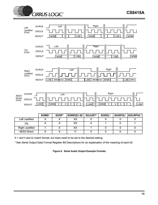
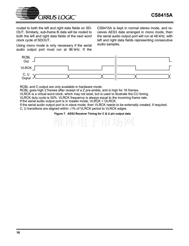
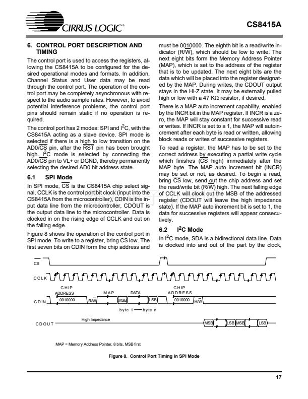
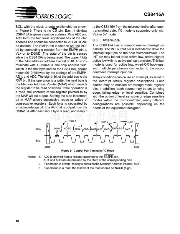
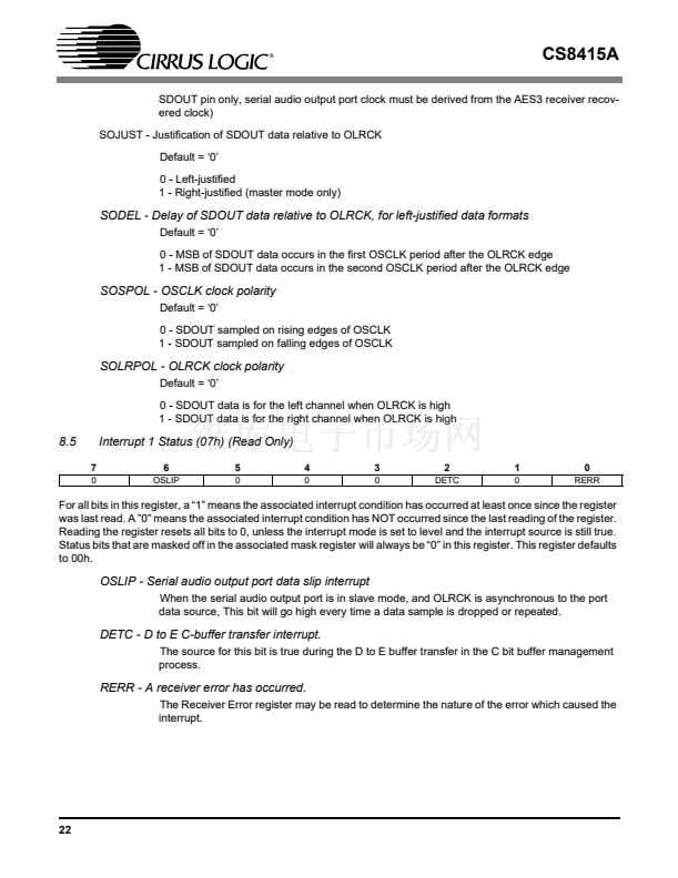
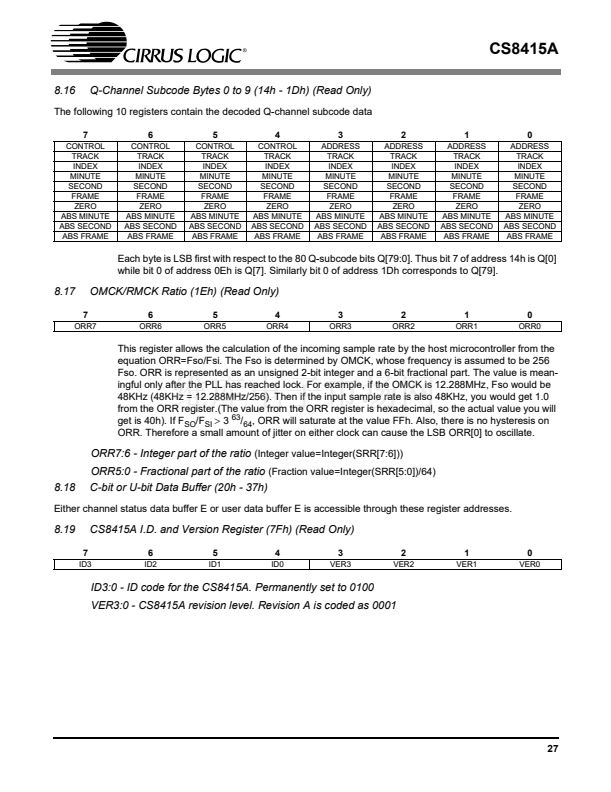
CS8415A
9. PIN DESCRIPTION - SOFTWARE MODE
SDA/CDOUT
AD0/CS
EMPH
RXP0
RXN0
VA+
AGND
FILT
RST
RMCK
RERR
RXP1
RXP2
RXP3
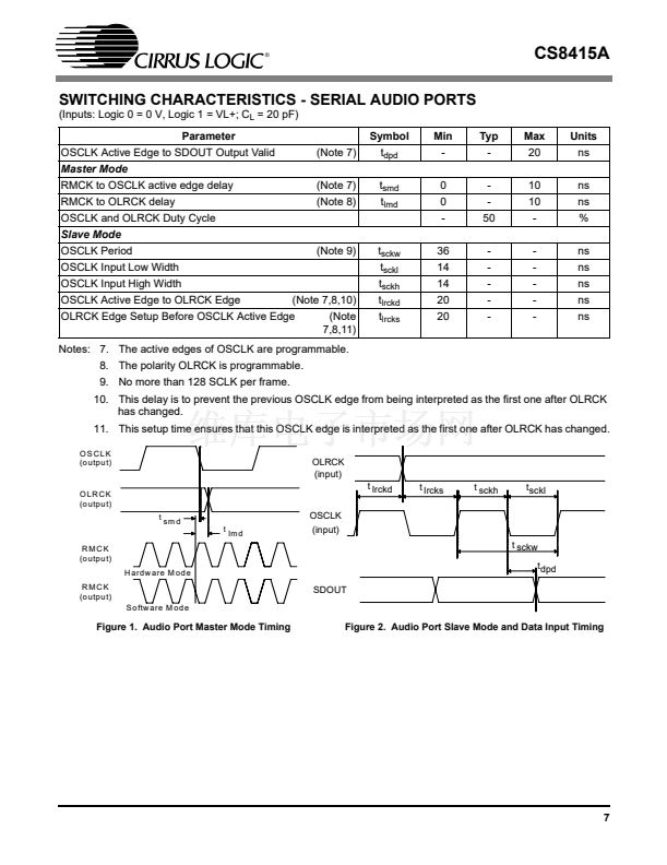
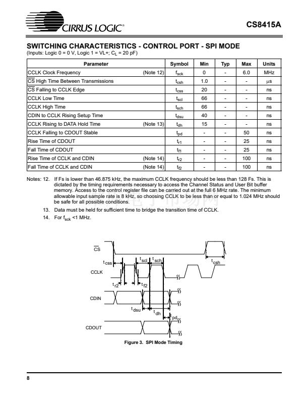
1
2
3*+
4*
5*
6*
7*
8*
9*
10*
11*
12
13
14
28
27
26
25
*24
*23
*22
*21
20
19
*18
*17
*16
15
SCL/CCLK
AD1/CDIN
RXP6
RXP5
H/S
VL+
DGND
OMCK
U
INT
SDOUT
OLRCK
OSCLK
RXP4
* Pins which remain the same function in all modes.
+ Pins which require a pull up or pull down resistor
to select the desired startup option.
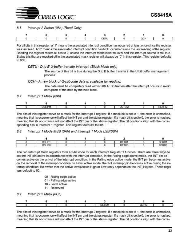
SDA/CDOUT
1
Serial Control Data I/O (I
2
C) / Data Out (SPI)
(Input/Output) - In I
2
C mode, SDA is the control I/O data
line. SDA is open drain and requires an external pull-up resistor to VL+. In SPI mode, CDOUT is the out-
put data from the control port interface on the CS8415A
Address Bit 0 (I
2
C) / Control Port Chip Select (SPI)
(Input) - A falling edge on this pin puts the
CS8415A into SPI control port mode. With no falling edge, the CS8415A defaults to I
2
C mode. In I
2
C
mode, AD0 is a chip address pin. In SPI mode, CS is used to enable the control port interface on the
CS8415A
Pre-Emphasis
(Output) - EMPH is low when the incoming Channel Status data indicates 50/15
碌s
pre-
emphasis. EMPH is high when the Channel Status data indicates no pre-emphasis or indicates pre-
emphasis other than 50/15
碌s.
This is also a start-up option pin, and requires a 47 k鈩?resistor to either
VL+ or DGND, which determines the AD2 address bit for the control port in I
2
C mode
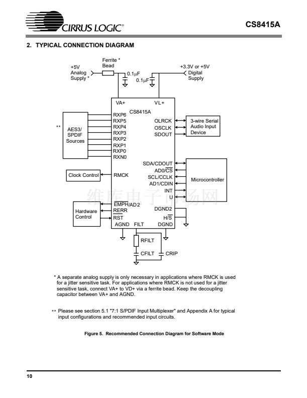
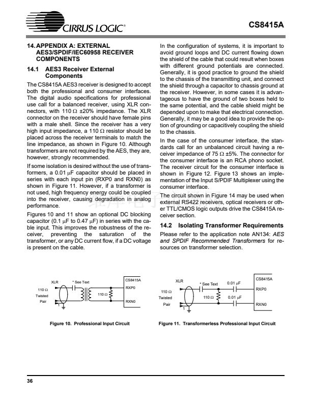
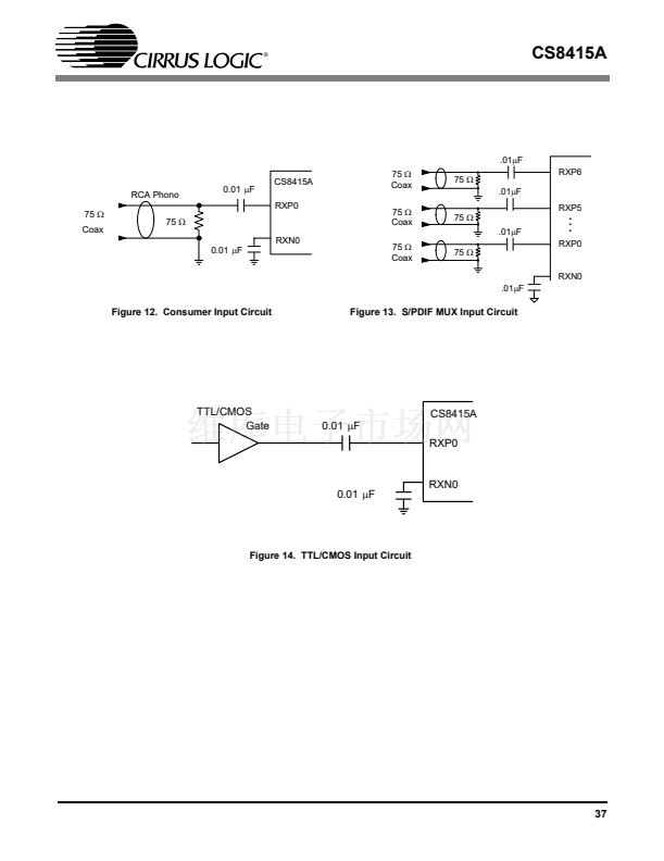
AES3/SPDIF Receiver Port
(Input) - Differential line receiver inputs carrying AES3 data. RXP0 may be
used as a single-ended input as part of 7:1 S/PDIF Input MUX. If RXP0 is used in MUX, RXN0 must be
ac coupled to ground.
Additional AES3/SPDIF Receiver Port
(Input) - Single-ended receiver inputs carrying AES3 or S/PDIF
digital data. These inputs, along with RXP0, comprise the 7:1 S/PDIF Input Multiplexer and select line
control is accessed using the MUX2:0 bits in the Control 2 register. Please note that any unused inputs
should be tied to ground. See Appendix A for recommended input circuits.
AD0/CS
2
EMPH
3
RXP0
RXN0
RXP1
RXP2
RXP3
RXP4
RXP5
RXP6
VA+
4
5
12
13
14
15
25
26
6
Positive Analog Power
(Input) - Positive supply for the analog section. Nominally +5 V. This supply
should be as quiet as possible since noise on this pin will directly affect the jitter performance of the
recovered clock
Analog Ground
(Input) - Ground for the analog circuitry in the chip. AGND and DGND should be con-
nected to a common ground area under the chip.
PLL Loop Filter
(Output) - An RC network should be connected between this pin and ground. See
鈥淎ppendix C: PLL Filter鈥?on page 40 for recommended schematic and component values.
Reset
(Input) - When RST is low, the CS8415A enters a low power mode and all internal states are
reset. On initial power up, RST must be held low until the power supply is stable, and all input clocks are
stable in frequency and phase. This is particularly true in hardware mode with multiple CS8415A devices
where synchronization between devices is important
AGND
FILT
RST
7
8
9
28


 1
1
 2
2
 3
3
 4
4
 5
5
 6
6
 7
7
 8
8
 9
9
 10
10
 11
11
 12
12
 13
13
 14
14
 15
15
 16
16
 17
17
 18
18
 19
19
 20
20
 21
21
 22
22
 23
23
 24
24
 25
25
 26
26
 27
27
 28
28
 29
29
 30
30
 31
31
 32
32
 33
33
 34
34
 35
35
 36
36
 37
37
 38
38
 39
39
 40
40
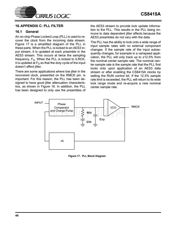
 41
41
 42
42
