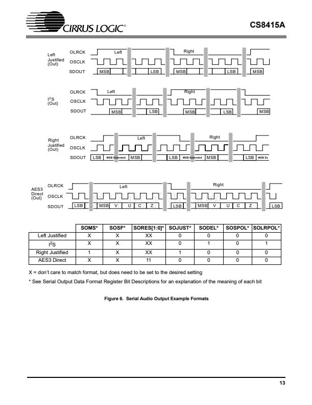
CS8415A
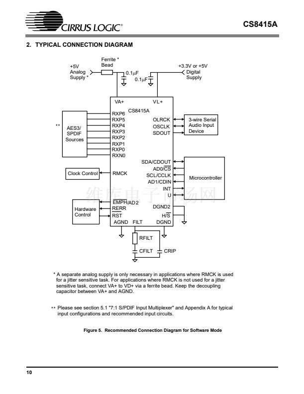
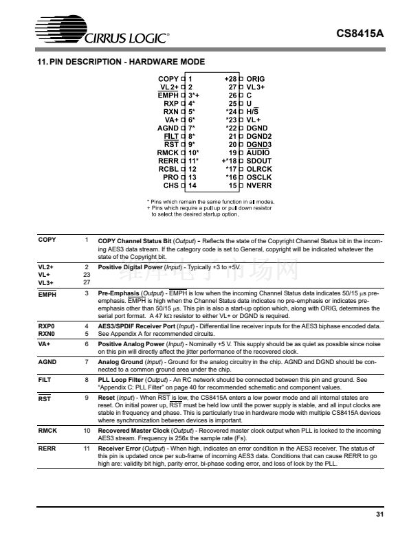
RMCK
RERR
10
11
Input Section Recovered Master Clock
(Output) - Input section recovered master clock output when
PLL is used. Frequency defaults to 256x the sample rate (Fs) and may be set to 128x.
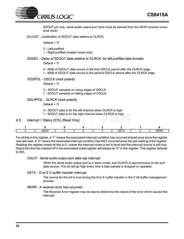
Receiver Error
(Output) - When high, indicates a problem with the operation of the AES3 receiver. The
status of this pin is updated once per sub-frame of incoming AES3 data. Conditions that can cause
RERR to go high are: validity, parity error, bi-phase coding error, confidence, QCRC and CCRC errors,
as well as loss of lock in the PLL. Each condition may be optionally masked from affecting the RERR pin
using the Receiver Error Mask Register. The RERR pin tracks the status of the unmasked errors: the pin
goes high as soon as an unmasked error occurs and goes low immediately when all unmasked errors go
away
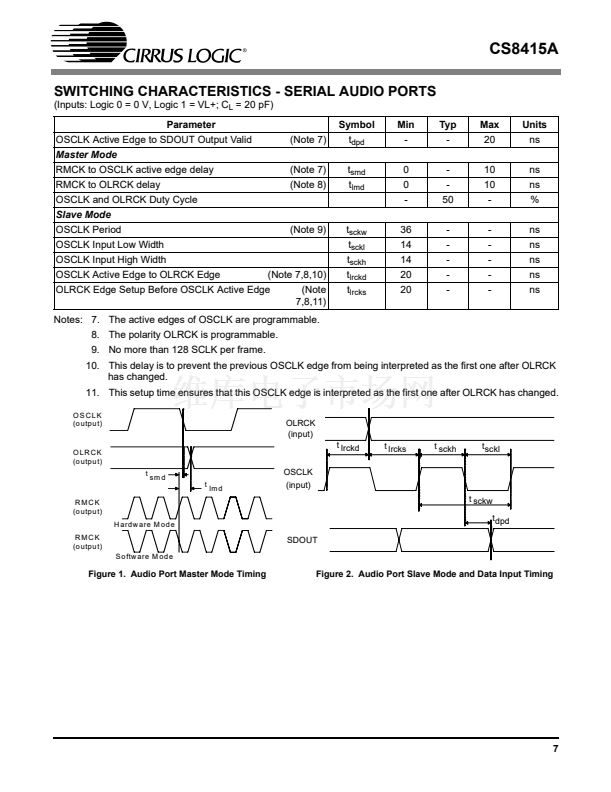
Serial Audio Output Bit Clock
(Input/Output) - Serial bit clock for audio data on the SDOUT pin
Serial Audio Output Left/Right Clock
(Input/Output) - Word rate clock for the audio data on the SDOUT
pin. Frequency will be the output sample rate (Fs)
Serial Audio Output Data
(Output) - Audio data serial output pin
Interrupt
(Output) - Indicates errors and key events during the operation of the CS8415A. All bits affect-
ing INT may be unmasked through bits in the control registers. The condition(s) that initiated interrupt are
readable through a control register. The polarity of the INT output, as well as selection of a standard or
open drain output, is set through a control register. Once set true, the INT pin goes false only after the
interrupt status registers have been read and the interrupt status bits have returned to zero
User Data
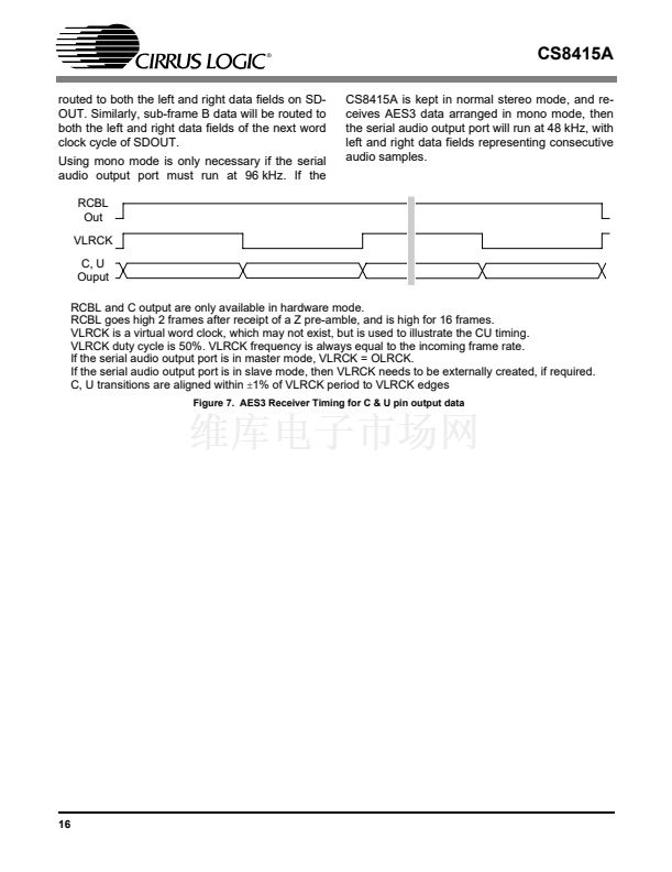
(Output) - Outputs User data from the AES3 receiver, see Figure 7 for timing information
System Clock
(Input) - When the OMCK System Clock Mode is enabled using the SWCLK bit in the
Control 1 register, the clock signal input on this pin is output through RMCK. OMCK serves as reference
signal for OMCK/RMCK ratio expressed in register 0x1E
Digital Ground
(Input) - Ground for the digital circuitry in the chip. DGND and AGND should be con-
nected to a common ground area under the chip.
Positive Digital Power
(Input) - Positive supply for the digital section. Typically +3 to +5 V.
Hardware/Software Mode Control
(Input) - Determines the method of controlling the operation of the
CS8415A, and the method of accessing CS and U data. In software mode, device control and CS and U
data access is primarily through the control port, using a microcontroller. Hardware mode provides an
alternate mode of operation and access to the CS and U data through dedicated pins. This pin should be
permanently tied to VL+ or DGND
Address Bit 1 (I
2
C) / Serial Control Data in (SPI)
(Input) - In I
2
C mode, AD1 is a chip address pin. In
SPI mode, CDIN is the input data line for the control port interface
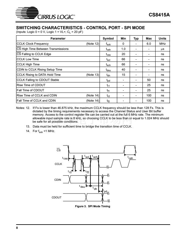
Control Port Clock
(Input) - Serial control interface clock and is used to clock control data bits into and
out of the CS8415A. In I
2
C mode, SCL requires an external pull-up resistor to VL+
OSCLK
OLRCK
SDOUT
INT
16
17
18
19
U
OMCK
20
21
DGND
VL+
H/S
22
23
24
AD1/CDIN
SCL/CCLK
27
28
29


 1
1
 2
2
 3
3
 4
4
 5
5
 6
6
 7
7
 8
8
 9
9
 10
10
 11
11
 12
12
 13
13
 14
14
 15
15
 16
16
 17
17
 18
18
 19
19
 20
20
 21
21
 22
22
 23
23
 24
24
 25
25
 26
26
 27
27
 28
28
 29
29
 30
30
 31
31
 32
32
 33
33
 34
34
 35
35
 36
36
 37
37
 38
38
 39
39
 40
40
 41
41
 42
42
