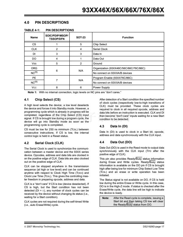
organization is selected. When it is connected to
ground, the (x8) organization is selected. Instruc-
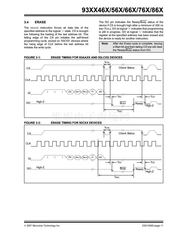
DI pin on the rising edge of the clock (CLK). The DO
Ready/Busy status during a programming operation.
DO high indicates the device is ready. DO will enter
the High-Z state on the falling edge of CS.
a typical voltage of 1.5V for 鈥?3AAXX鈥?and 鈥?3LCXX鈥?/div>
devices or 3.8V for 鈥?3CXX鈥?devices.
The EWEN and EWDS commands give additional
protection against accidentally programming during
normal operation.
Note:
For added protection, an EWDS command
should be performed after every write
operation and an external 10 k惟 pull-down
protection resistor should be added to the
CS pin.
3.1
Start Condition
The Start bit is detected by the device if CS and DI are
both high with respect to the positive edge of CLK for
the first time.
Before a Start condition is detected, CS, CLK and DI
may change in any combination (except to that of a
Start condition), without resulting in any device
operation (Read, Write, Erase, EWEN, EWDS, ERAL
or WRAL). As soon as CS is high, the device is no
longer in Standby mode.
An instruction following a Start condition will only be
executed if the required opcode, address and data bits
for any particular instruction are clocked in.
Note:
When preparing to transmit an instruction,
either the CLK or DI signal levels must be
at a logic low as CS is toggled active high.
After power-up, the device is automatically in the
EWDS mode. Therefore, an
EWEN
instruction must be
performed before the initial
ERASE
or
WRITE
instruction
can be executed.
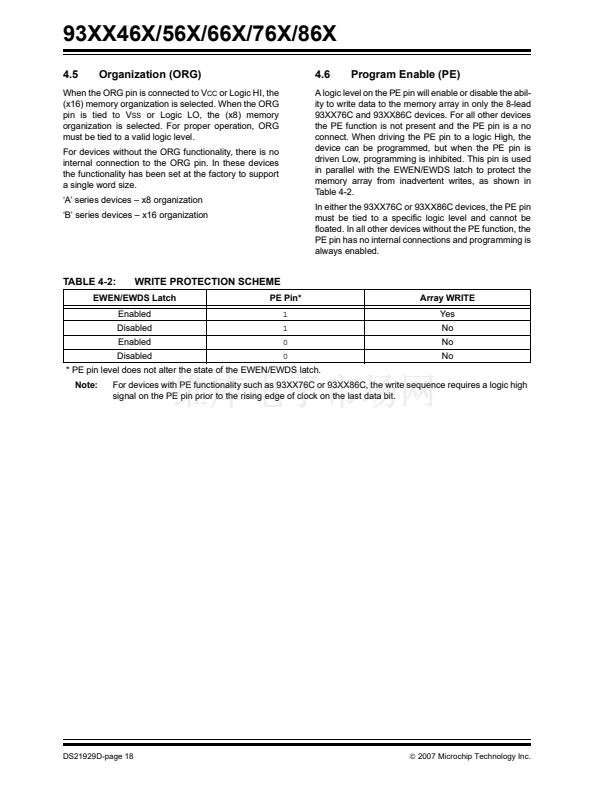
Note:
To prevent accidental writes to the array in
the 93XX76C/86C devices, set the PE pin
to a logic low.
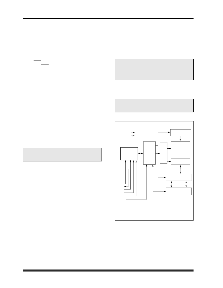
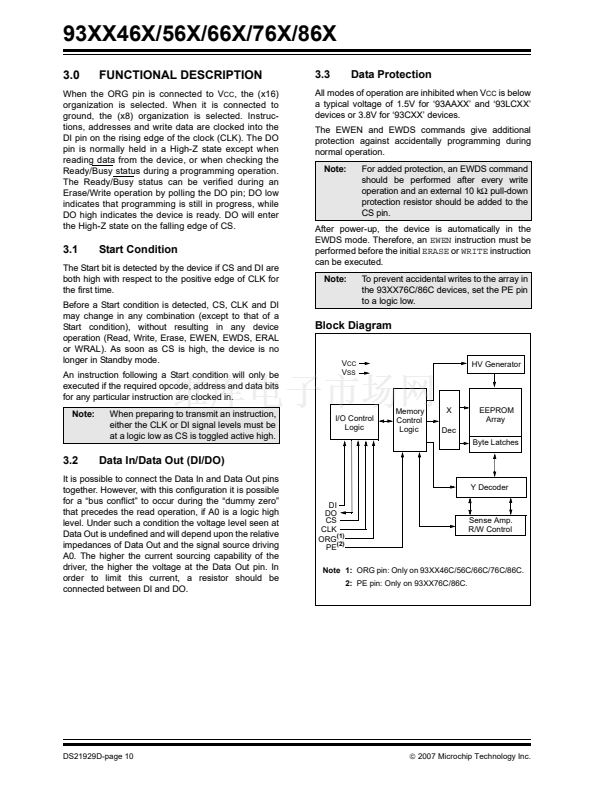
Block Diagram
V
CC
V
SS
HV Generator
I/O Control
Logic
Memory
Control
Logic
X
Dec
EEPROM
Array
Byte Latches
3.2
Data In/Data Out (DI/DO)
Y Decoder
DI
DO
CS
CLK
ORG
(1)
PE
(2)
It is possible to connect the Data In and Data Out pins
together. However, with this configuration it is possible
for a 鈥渂us conflict鈥?to occur during the 鈥渄ummy zero鈥?/div>
that precedes the read operation, if A0 is a logic high
level. Under such a condition the voltage level seen at
Data Out is undefined and will depend upon the relative
impedances of Data Out and the signal source driving
A0. The higher the current sourcing capability of the
driver, the higher the voltage at the Data Out pin. In
order to limit this current, a resistor should be
connected between DI and DO.
Sense Amp.
R/W Control
Note 1:
ORG pin: Only on 93XX46C/56C/66C/76C/86C.
2:
PE pin: Only on 93XX76C/86C.
DS21929D-page 10
漏
2007 Microchip Technology Inc.


 1
1
 2
2
 3
3
 4
4
 5
5
 6
6
 7
7
 8
8
 9
9
 10
10
 11
11
 12
12
 13
13
 14
14
 15
15
 16
16
 17
17
 18
18
 19
19
 20
20
 21
21
 22
22
 23
23
 24
24
 25
25
 26
26
 27
27
 28
28
 29
29
 30
30
 31
31
 32
32
 33
33
 34
34
 35
35
 36
36
 37
37
 38
38
