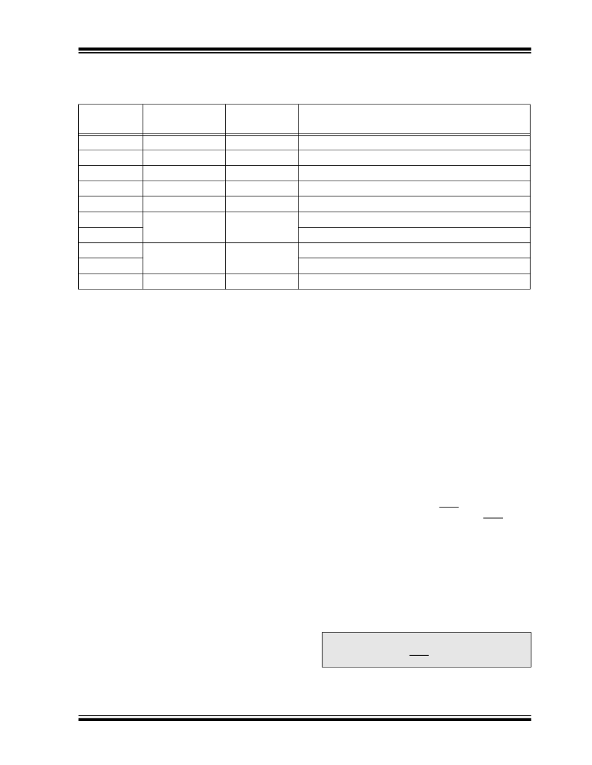
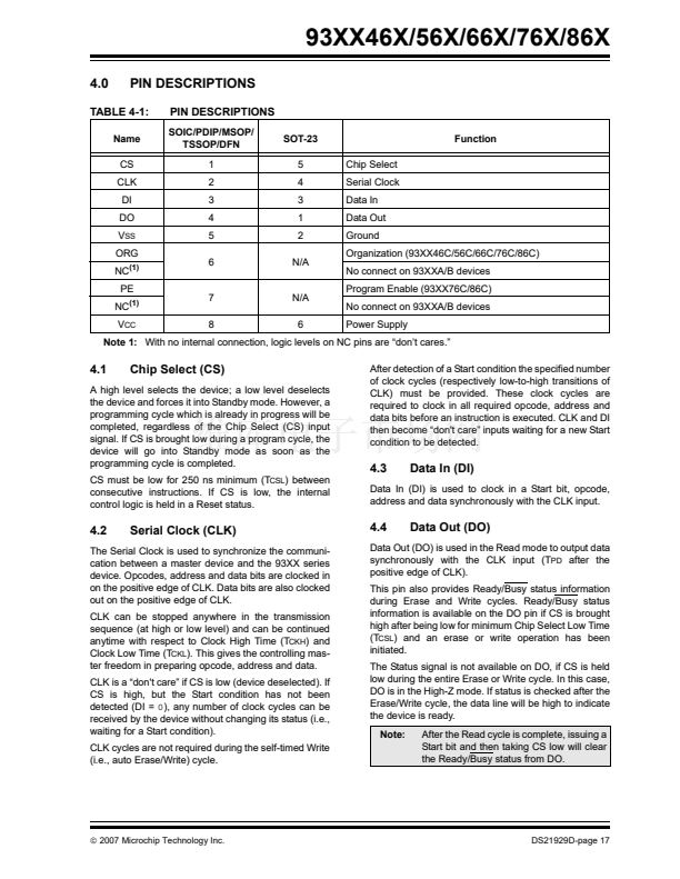
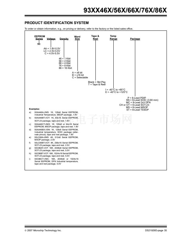
With no internal connection, logic levels on NC pins are 鈥渄on鈥檛 cares.鈥?/div>
4.1
Chip Select (CS)
A high level selects the device; a low level deselects
the device and forces it into Standby mode. However, a
programming cycle which is already in progress will be
completed, regardless of the Chip Select (CS) input
signal. If CS is brought low during a program cycle, the
device will go into Standby mode as soon as the
programming cycle is completed.
CS must be low for 250 ns minimum (T
CSL
) between
consecutive instructions. If CS is low, the internal
control logic is held in a Reset status.
After detection of a Start condition the specified number
of clock cycles (respectively low-to-high transitions of
CLK) must be provided. These clock cycles are
required to clock in all required opcode, address and
data bits before an instruction is executed. CLK and DI
then become 鈥渄on't care鈥?inputs waiting for a new Start
condition to be detected.
4.3
Data In (DI)
Data In (DI) is used to clock in a Start bit, opcode,
address and data synchronously with the CLK input.
4.2
Serial Clock (CLK)
4.4
Data Out (DO)
The Serial Clock is used to synchronize the communi-
cation between a master device and the 93XX series
device. Opcodes, address and data bits are clocked in
on the positive edge of CLK. Data bits are also clocked
out on the positive edge of CLK.
CLK can be stopped anywhere in the transmission
sequence (at high or low level) and can be continued
anytime with respect to Clock High Time (T
CKH
) and
Clock Low Time (T
CKL
). This gives the controlling mas-
ter freedom in preparing opcode, address and data.
CLK is a 鈥渄on't care鈥?if CS is low (device deselected). If
CS is high, but the Start condition has not been
detected (DI =
0),
any number of clock cycles can be
received by the device without changing its status (i.e.,
waiting for a Start condition).
CLK cycles are not required during the self-timed Write
(i.e., auto Erase/Write) cycle.
Data Out (DO) is used in the Read mode to output data
synchronously with the CLK input (T
PD
after the
positive edge of CLK).
This pin also provides Ready/Busy status information
during Erase and Write cycles. Ready/Busy status
information is available on the DO pin if CS is brought
high after being low for minimum Chip Select Low Time
(T
CSL
) and an erase or write operation has been
initiated.
The Status signal is not available on DO, if CS is held
low during the entire Erase or Write cycle. In this case,
DO is in the High-Z mode. If status is checked after the
Erase/Write cycle, the data line will be high to indicate
the device is ready.
Note:
After the Read cycle is complete, issuing a
Start bit and then taking CS low will clear
the Ready/Busy status from DO.
漏
2007 Microchip Technology Inc.
DS21929D-page 17


 1
1
 2
2
 3
3
 4
4
 5
5
 6
6
 7
7
 8
8
 9
9
 10
10
 11
11
 12
12
 13
13
 14
14
 15
15
 16
16
 17
17
 18
18
 19
19
 20
20
 21
21
 22
22
 23
23
 24
24
 25
25
 26
26
 27
27
 28
28
 29
29
 30
30
 31
31
 32
32
 33
33
 34
34
 35
35
 36
36
 37
37
 38
38
