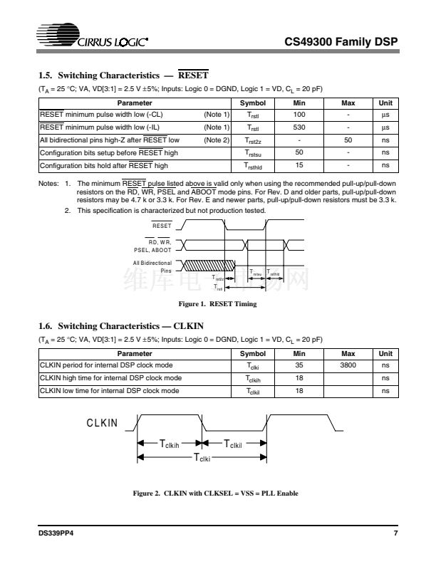
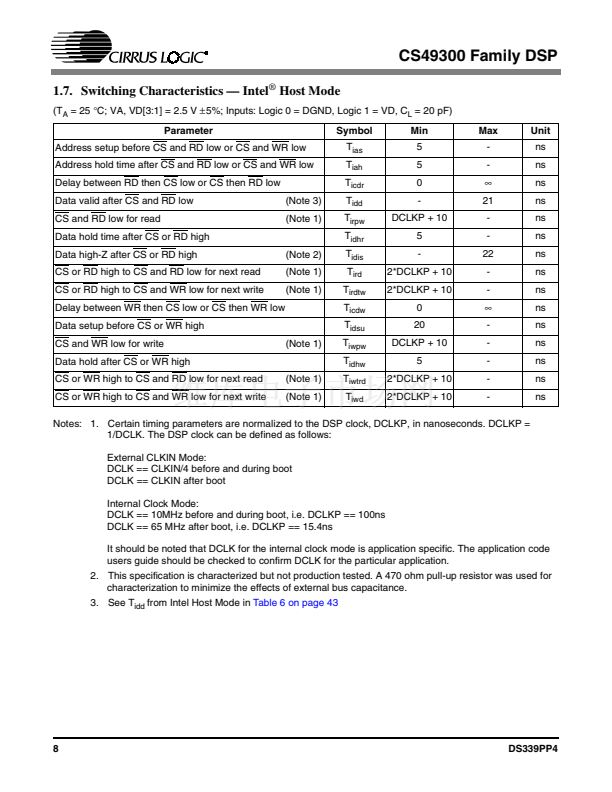
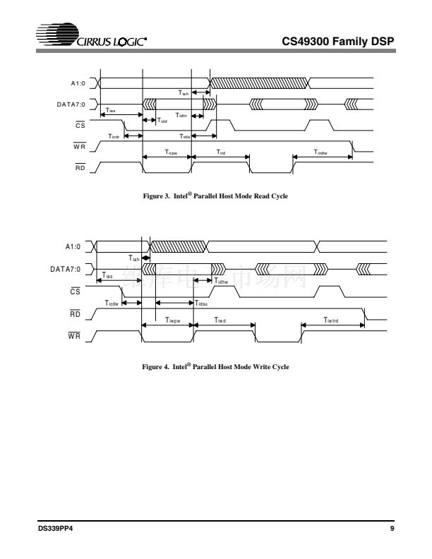
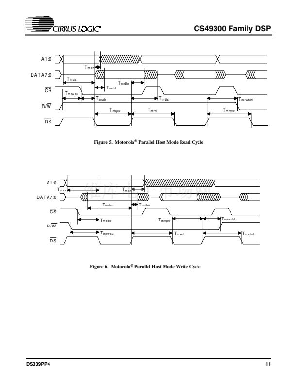
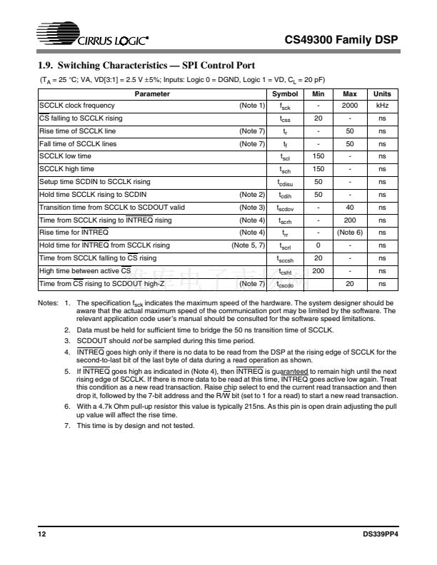
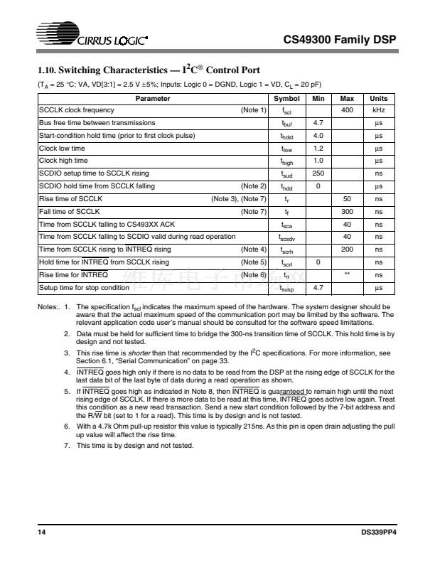
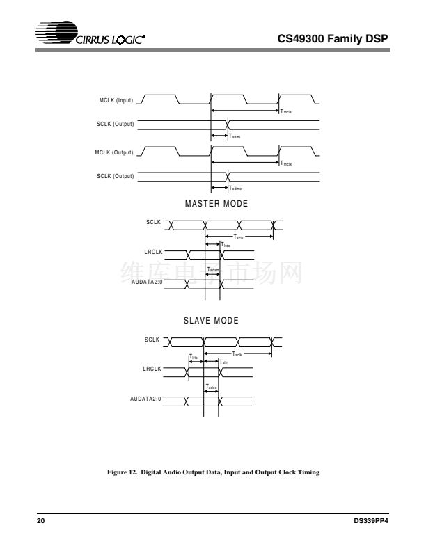
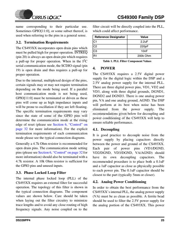
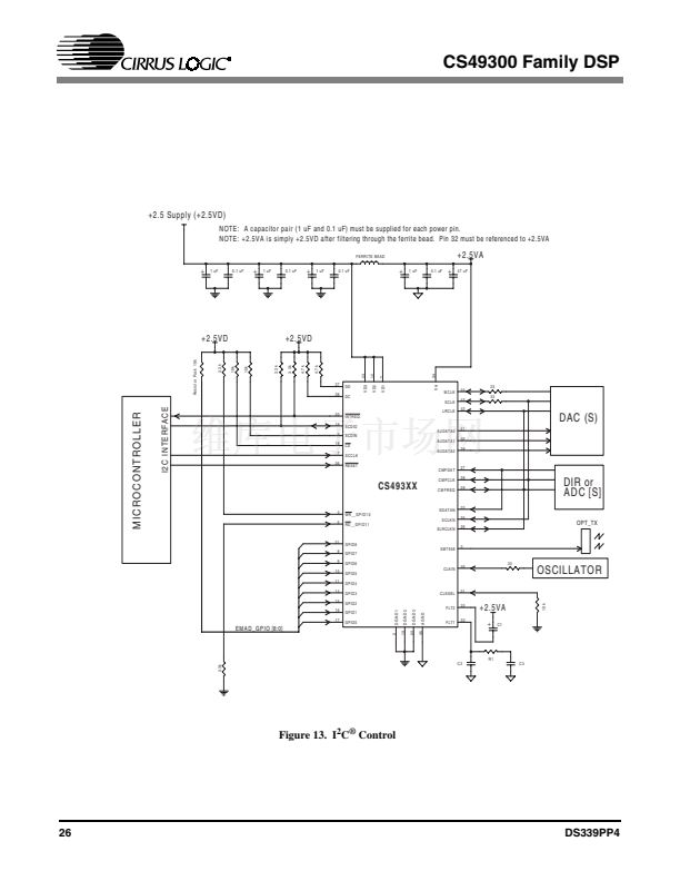
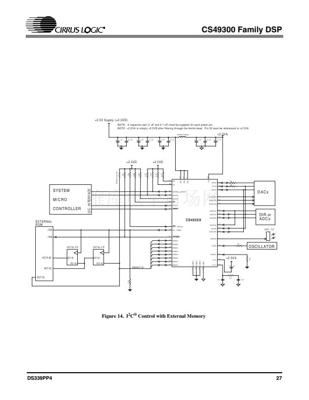
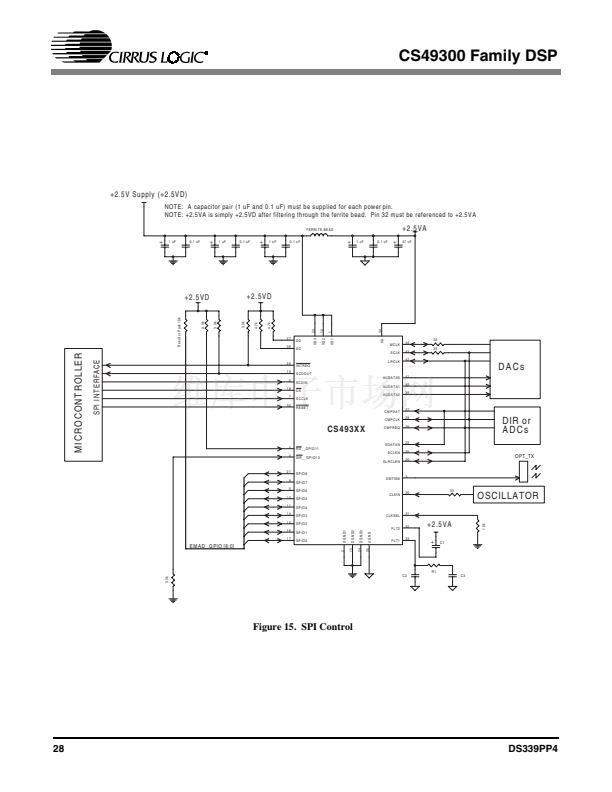
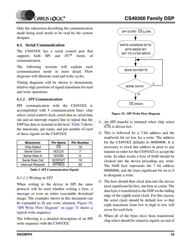
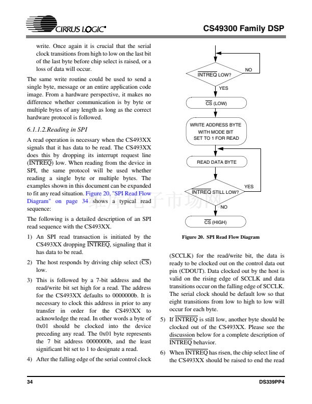
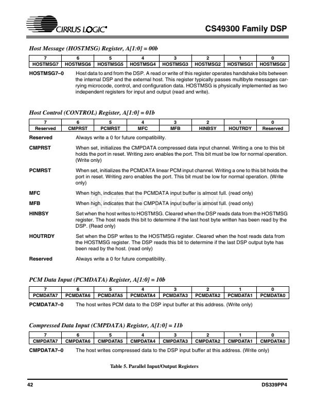
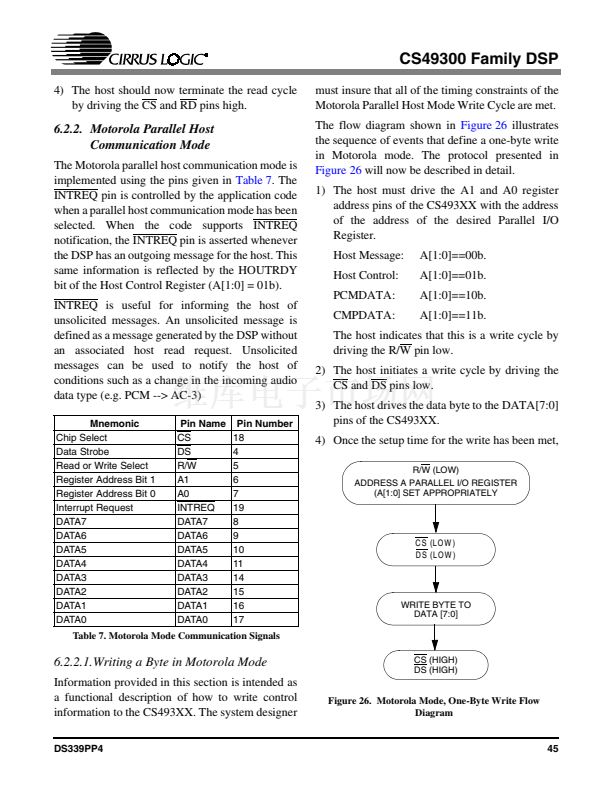
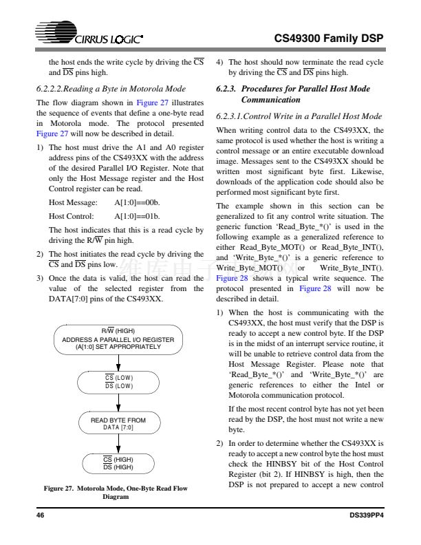
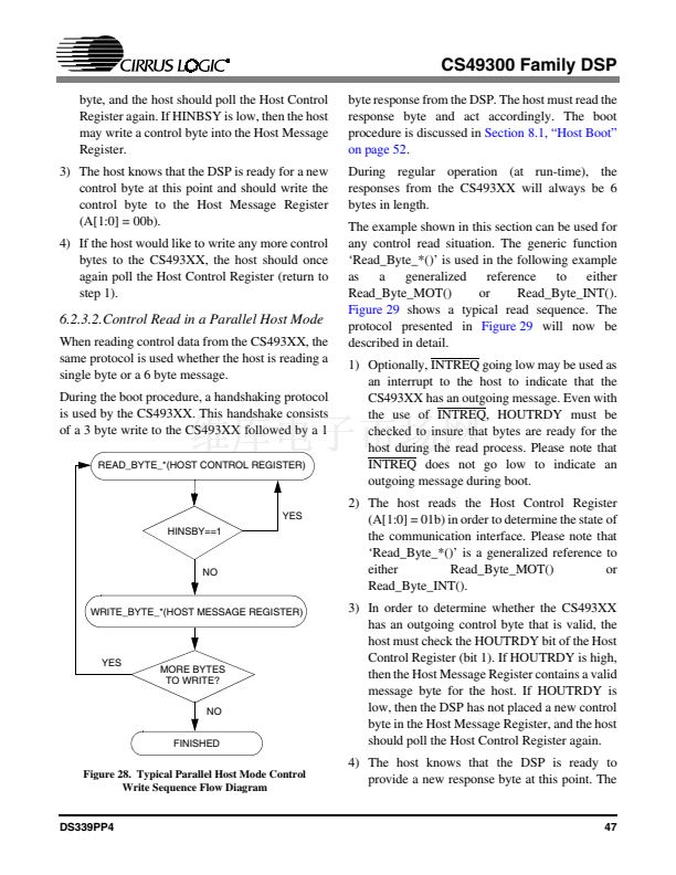
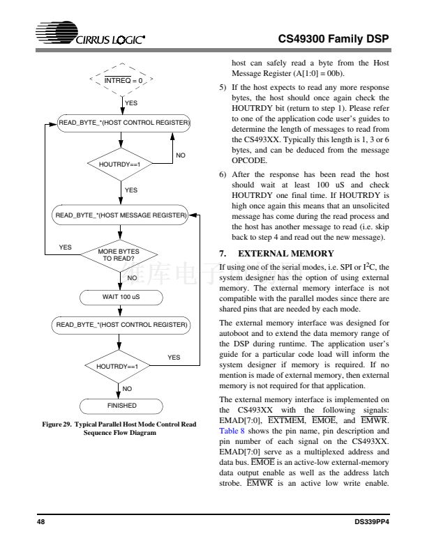
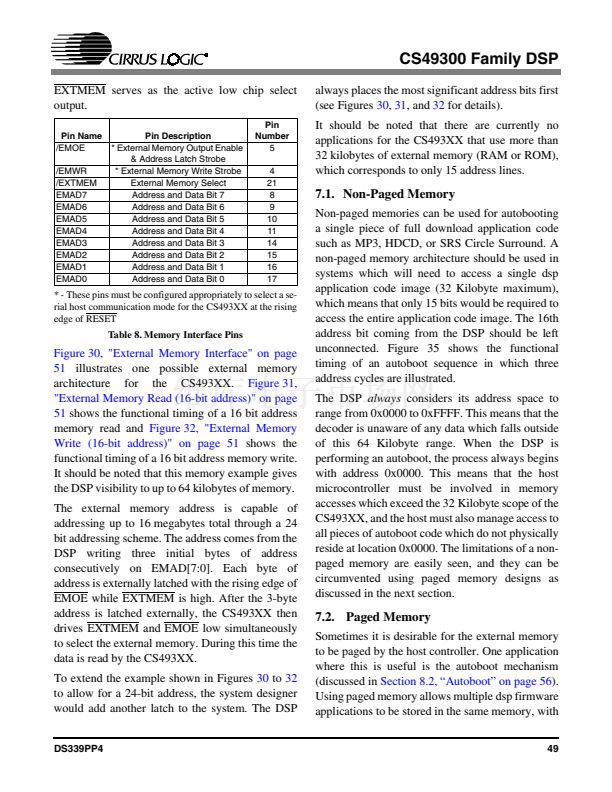
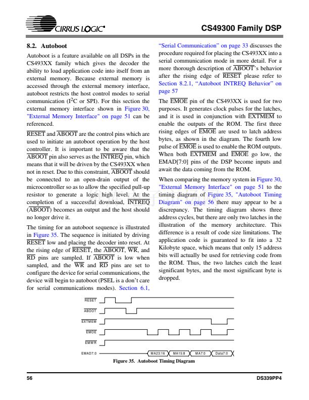
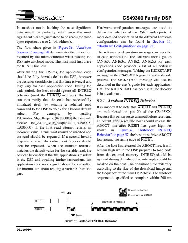
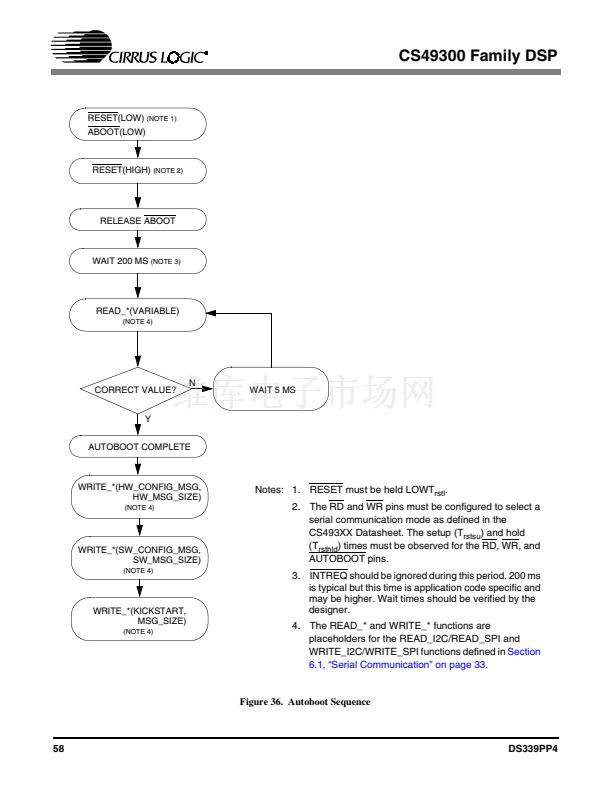
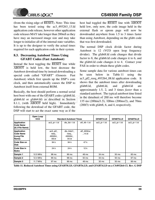
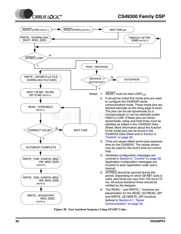
CS49300 Family DSP
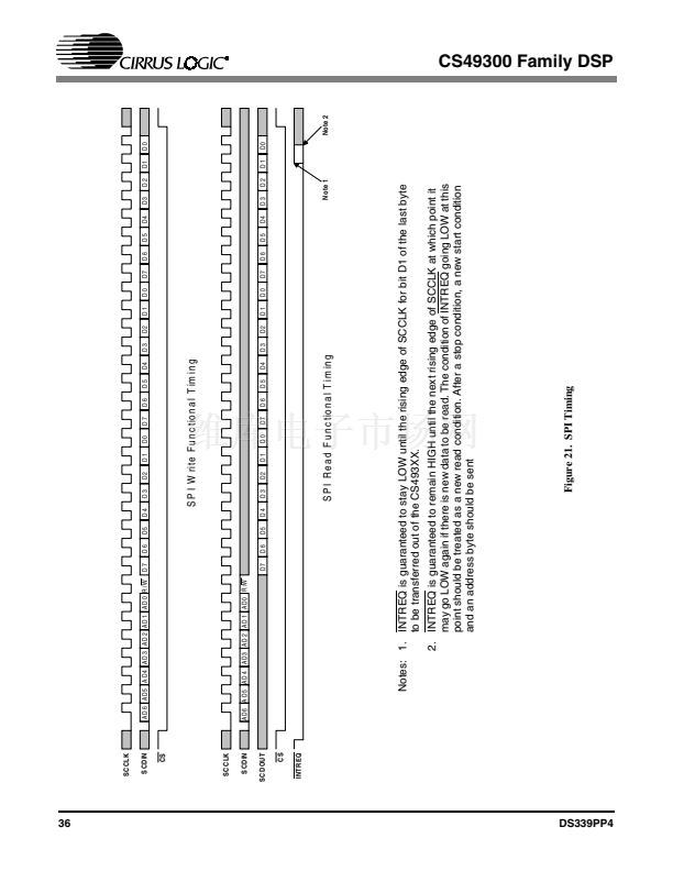
transaction.
Understanding the role of INTREQ is important for
successful communication. INTREQ is guaranteed
to remain low (once it has gone low) until the
second to last rising edge of SCCLK of the last byte
to be transferred out of the CS493XX. If there is no
more data to be transferred, INTREQ will go high
at this point. For SPI this is the rising edge for the
second to last bit of the last byte to be transferred.
After going high, INTREQ is guaranteed to stay
high until the next rising edge of SCCLK. This end
of transfer condition signals the host to end the read
transaction by clocking the last data bit out and
raising CS. If INTREQ is still low after the second
to last rising edge of SCCLK, the host should
continue reading data from the serial control port.
It should be noted that all data should be read out of
the serial control port during one cycle or a loss of
data will occur. In other words, all data should be
read out of the chip until INTREQ signals the last
byte by going high as described above. Please see
Section 6.1.3, 鈥淚NTREQ Behavior: A Special
Case鈥?on page 39
for a more detailed description of
INTREQ behavior.
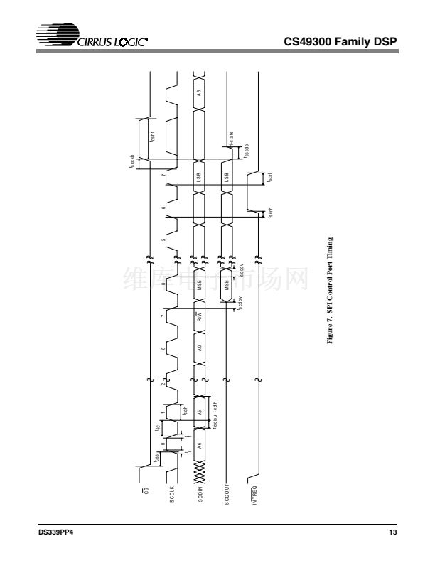
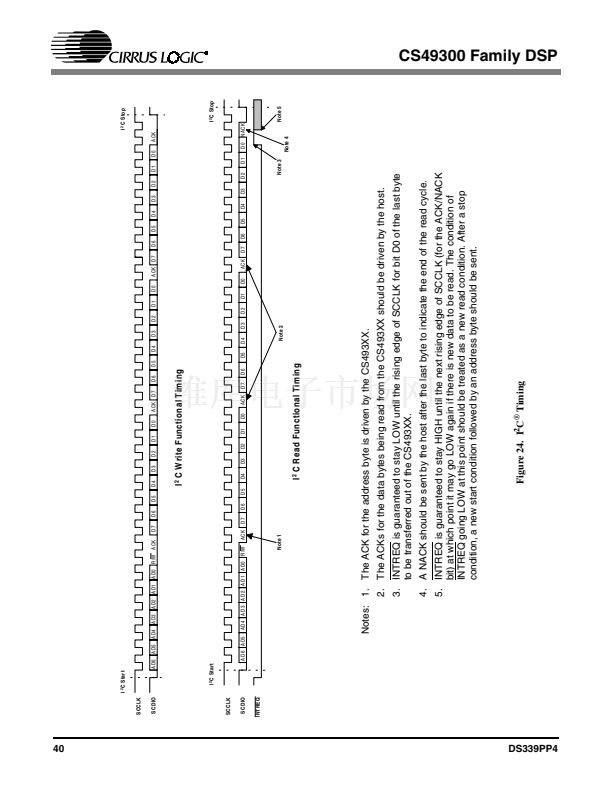
Figure 21, "SPI Timing" on page 36
timing
diagram shows the relative edges of the control
lines for an SPI read and write.
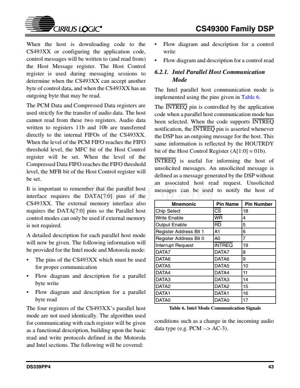
page 35 shows the mnemonic, pin name, and pin
number of each of these signals on the CS493XX.
Mnemonic
Serial Clock
Bi-Directional Data
Interrupt Request
Pin Name
SCCLK
SCDIO
INTREQ
Pin Number
7
19
20
Table 4. I
2
C
庐
Communication Signals
Typically in I
2
C
庐
communication SCDIO is an
open drain line with a pull-up. A logic one is placed
on the line by three-stating the output and allowing
the pull-up to raise the line. At this point another
device can drive the line low if necessary. Three-
stating SCDIO can have two effects: 1. To send out
a one when writing data or sending a 鈥渘o
acknowledge鈥? 2. release the line when another
chip is writing data.
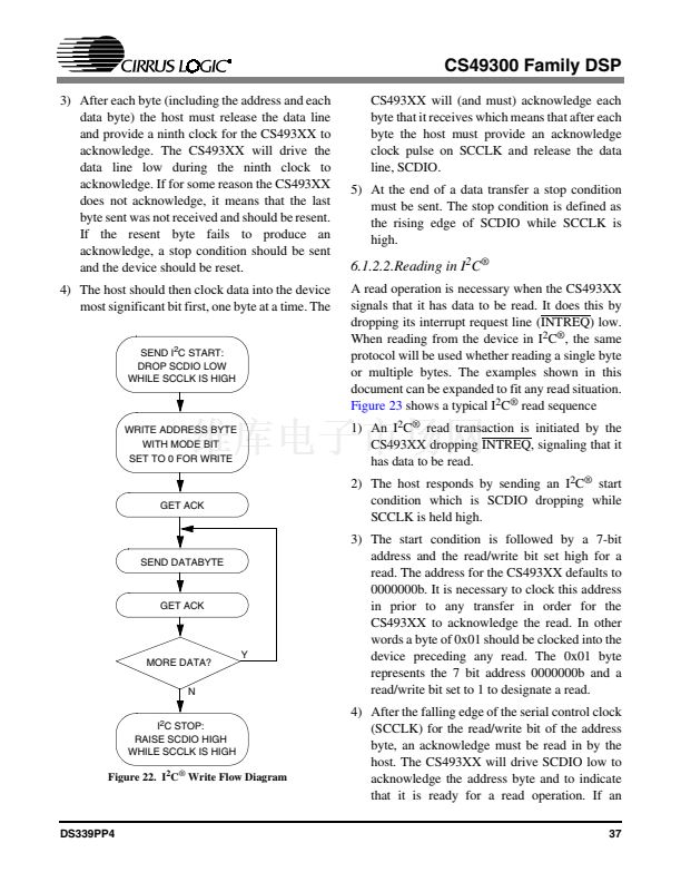
6.1.2.1.Writing in I
2
C
庐
When writing to the device in I
2
C
庐
the same
protocol will be used whether writing a byte, a
message or even an application code image. The
examples shown in this document can be expanded
to fit any write situation.
Figure 23
shows a typical
write sequence:
The following is a detailed description of an I
2
C
庐
write sequence with the CS493XX.
1) An I
2
C
庐
transfer is initiated with an I
2
C
庐
start
condition which is defined as the data (SCDIO)
line falling while the clock (SCCLK) is held
high.
2) Next a 7-bit address with the read/write bit set
low for a write should be sent to the CS493XX.
The address for the CS493XX defaults to
0000000b. It is necessary to clock this address
in prior to any transfer in order for the
CS493XX to accept the write. In other words a
byte of 0x00 should be clocked into the device
preceding any write. The 0x00 byte represents
the 7 bit of address (0000000b) and the
read/write bit set to 0 to designate a write.
35
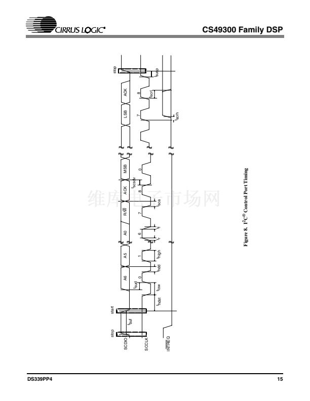
6.1.2. I C Communication
I
2
C communication with the CS493XX is
accomplished with 3 communication lines: serial
control clock, a bi-directional serial data
input/output line and an interrupt request line to
signal that the DSP has data to transmit to the host.
See Figure 4, "I
2
C庐 Communication Signals" on
2
DS339PP4


 1
1
 2
2
 3
3
 4
4
 5
5
 6
6
 7
7
 8
8
 9
9
 10
10
 11
11
 12
12
 13
13
 14
14
 15
15
 16
16
 17
17
 18
18
 19
19
 20
20
 21
21
 22
22
 23
23
 24
24
 25
25
 26
26
 27
27
 28
28
 29
29
 30
30
 31
31
 32
32
 33
33
 34
34
 35
35
 36
36
 37
37
 38
38
 39
39
 40
40
 41
41
 42
42
 43
43
 44
44
 45
45
 46
46
 47
47
 48
48
 49
49
 50
50
 51
51
 52
52
 53
53
 54
54
 55
55
 56
56
 57
57
 58
58
 59
59
 60
60
 61
61
 62
62
 63
63
 64
64
 65
65
 66
66
 67
67
 68
68
 69
69
 70
70
 71
71
 72
72
 73
73
 74
74
 75
75
 76
76
 77
77
 78
78
 79
79
 80
80
 81
81
 82
82
 83
83
 84
84
 85
85
 86
86
