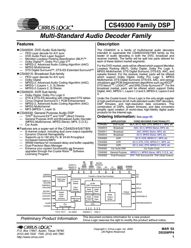
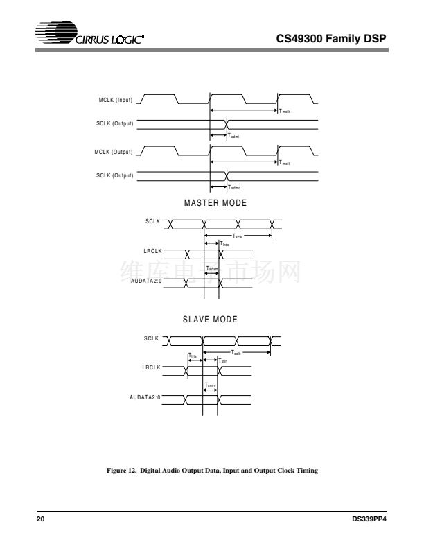
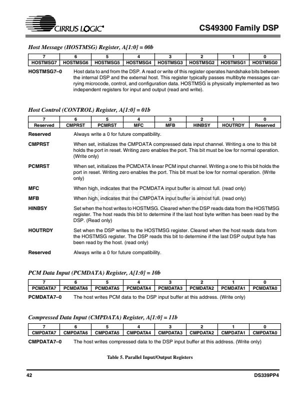
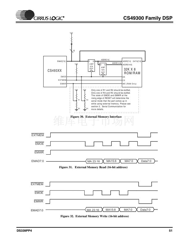
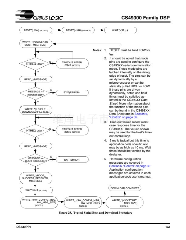
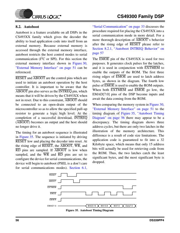
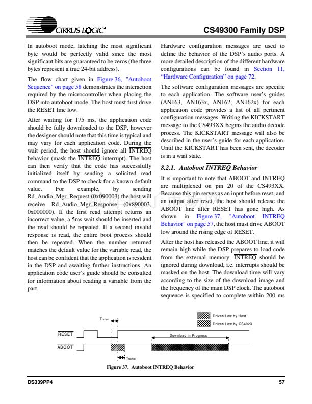
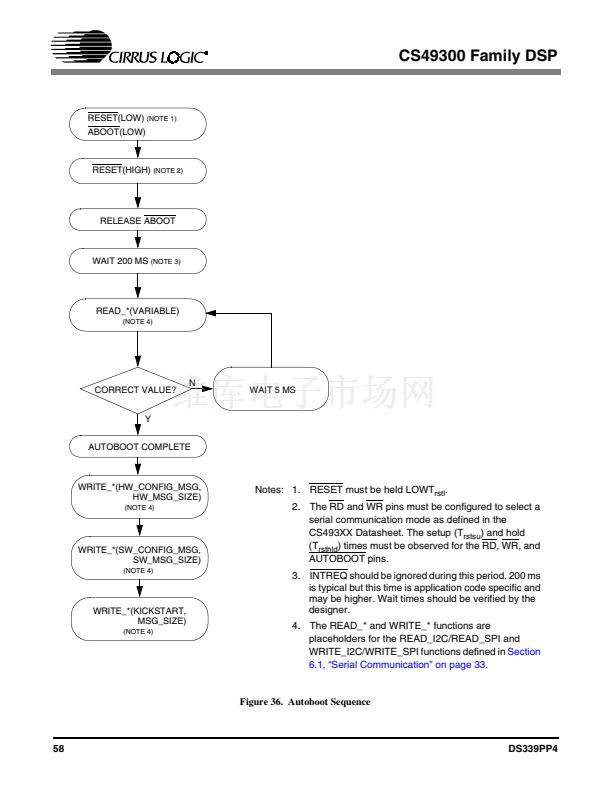
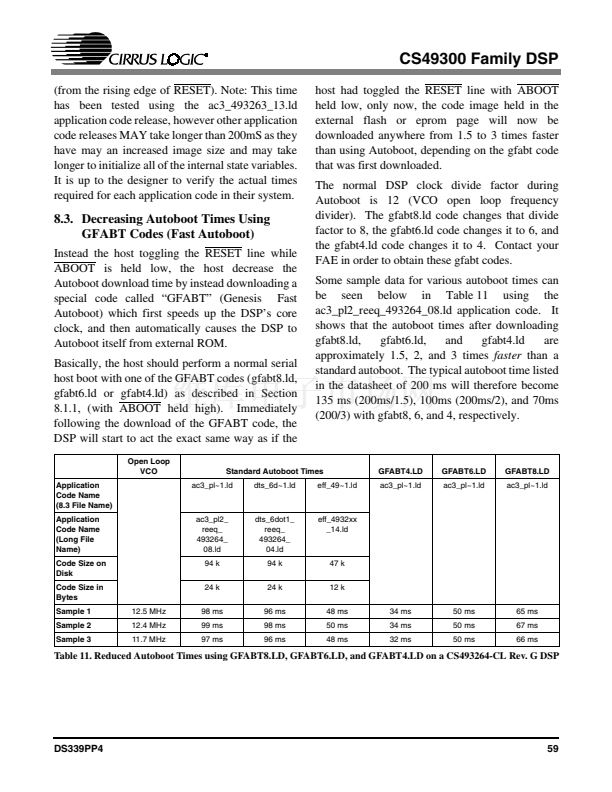
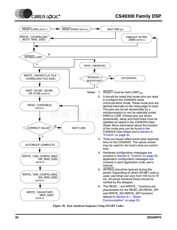
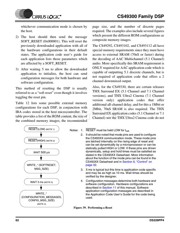
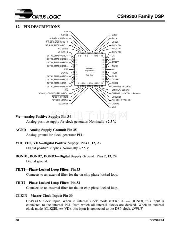
CS49300 Family DSP
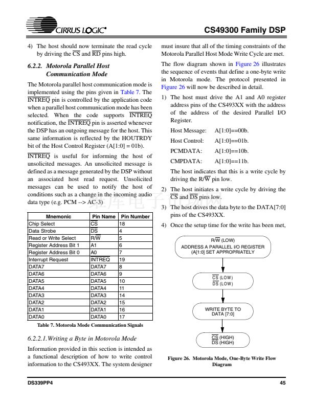
When the host is downloading code to the
CS493XX or configuring the application code,
control messages will be written to (and read from)
the Host Message register. The Host Control
register is used during messaging sessions to
determine when the CS493XX can accept another
byte of control data, and when the CS493XX has an
outgoing byte that may be read.
The PCM Data and Compressed Data registers are
used strictly for the transfer of audio data. The host
cannot read from these two registers. Audio data
written to registers 11b and 10b are transferred
directly to the internal FIFOs of the CS493XX.
When the level of the PCM FIFO reaches the FIFO
threshold level, the MFC bit of the Host Control
register will be set. When the level of the
Compressed Data FIFO reaches the FIFO threshold
level, the MFB bit of the Host Control register will
be set.
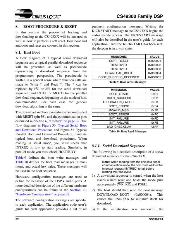
It is important to remember that the parallel host
interface requires the DATA[7:0] pins of the
CS493XX. The external memory interface also
requires the DATA[7:0] pins so the Parallel host
control modes can only be used if external memory
is not required.
A detailed description for each parallel host mode
will now be given. The following information will
be provided for the Intel mode and Motorola mode:
The pins of the CS493XX which must be used
for proper communication
鈥?Flow diagram and description for a parallel
byte write
鈥?Flow diagram and description for a parallel
byte read
The four registers of the CS493XX鈥檚 parallel host
mode are not used identically. The algorithm used
for communicating with each register will be given
as a functional description, building upon the basic
read and write protocols defined in the Motorola
and Intel sections. The following will be covered:
鈥?/div>
鈥?/div>
鈥?/div>
Flow diagram and description for a control
write
Flow diagram and description for a control read
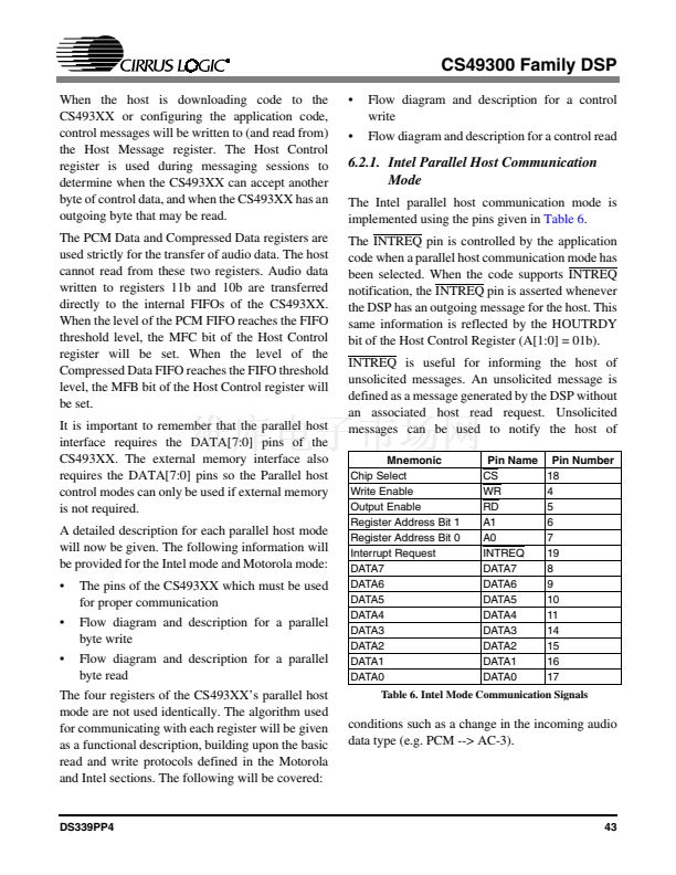
6.2.1. Intel Parallel Host Communication
Mode
The Intel parallel host communication mode is
implemented using the pins given in
Table 6.
The INTREQ pin is controlled by the application
code when a parallel host communication mode has
been selected. When the code supports INTREQ
notification, the INTREQ pin is asserted whenever
the DSP has an outgoing message for the host. This
same information is reflected by the HOUTRDY
bit of the Host Control Register (A[1:0] = 01b).
INTREQ is useful for informing the host of
unsolicited messages. An unsolicited message is
defined as a message generated by the DSP without
an associated host read request. Unsolicited
messages can be used to notify the host of
Mnemonic
Chip Select
Write Enable
Output Enable
Register Address Bit 1
Register Address Bit 0
Interrupt Request
DATA7
DATA6
DATA5
DATA4
DATA3
DATA2
DATA1
DATA0
Pin Name
CS
WR
RD
A1
A0
INTREQ
DATA7
DATA6
DATA5
DATA4
DATA3
DATA2
DATA1
DATA0
Pin Number
18
4
5
6
7
19
8
9
10
11
14
15
16
17
Table 6. Intel Mode Communication Signals
conditions such as a change in the incoming audio
data type (e.g. PCM --> AC-3).
DS339PP4
43


 1
1
 2
2
 3
3
 4
4
 5
5
 6
6
 7
7
 8
8
 9
9
 10
10
 11
11
 12
12
 13
13
 14
14
 15
15
 16
16
 17
17
 18
18
 19
19
 20
20
 21
21
 22
22
 23
23
 24
24
 25
25
 26
26
 27
27
 28
28
 29
29
 30
30
 31
31
 32
32
 33
33
 34
34
 35
35
 36
36
 37
37
 38
38
 39
39
 40
40
 41
41
 42
42
 43
43
 44
44
 45
45
 46
46
 47
47
 48
48
 49
49
 50
50
 51
51
 52
52
 53
53
 54
54
 55
55
 56
56
 57
57
 58
58
 59
59
 60
60
 61
61
 62
62
 63
63
 64
64
 65
65
 66
66
 67
67
 68
68
 69
69
 70
70
 71
71
 72
72
 73
73
 74
74
 75
75
 76
76
 77
77
 78
78
 79
79
 80
80
 81
81
 82
82
 83
83
 84
84
 85
85
 86
86
